|
|
Early Bird Registration Is Now Open! The 14th International System-on-Chip (SoC) Conference, Exhibit & Workshops October 19 & 20, 2016 University of California, Irvine (UCI) - Calit2 |
|
||
|
|
SoC Conference Platinum Sponsors
|
||||||||||
|
|
3rd
International System-on-Chip (SoC)
Conference & exhibit Detailed Program Information (Abstracts & Bios) for Tuesday, November 1, 2005* |
|
|
|
|
|
|
|
 8:00 am - 8:15 am |
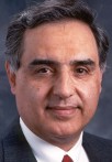
 Farhad
Mafie, President and CEO of Savant Company Inc. Farhad
Mafie, President and CEO of Savant Company Inc.
"Welcome and Opening Remarks, Technology/Market Trends." Farhad has over 20 years of experience in semiconductor and computer businesses and more than 10 years of university-level teaching experience. Farhad is the former Vice President of Marketing/Business Development and Technical Sales Engineering at Toshiba America Electronic Components, Inc. He was responsible for marketing the entire Toshiba standard ICs (RISC/CISC CPUs, Configurable CPUs, DSPs, Bluetooth, Wireless ICs, RFID, MPEG-4, CCD/CMOS, Analog ICs, Automotive ICs, etc.). He was also responsible for engineering development for Toshiba's Embedded and Digital Consumer products & solutions based on ASSP and SoC Models. Farhad established Toshiba's on-line Tech-Support System as well as Toshiba's on-line System Solution Selling methodologies for all Toshiba's products in the North American markets. These on-line systems were adopted by Toshiba on a worldwide basis. He also developed Toshiba's ASSP Business Unit and Technical Sales Engineering Team as two brand new organizations for the company. Farhad has also worked at Lucent Technologies on marketing communications ICs, Toshiba Information Systems on product definition for Toshiba's notebooks and handheld products, Unisys on designing new processors and computer systems, and MSI Data on designing data collection products. He has a Master of Science and a Bachelor of Science degree in Electronic Engineering from California State University, Fullerton. His combined business and academic experience has given Farhad a unique ability to effectively communicate complex new technologies to business professionals at all levels, as well as the ability to foresee emerging leading-edge technologies. Farhad is an author and a translator, and he writes articles for a variety of journals and Web-based magazines on technology and political affairs.
|
|
8:15 am- 8:45 am Keynote |
 Derek Lidow, CEO and President, iSuppli "New Realities Mandate Fundamental Changes in Competitive Strategies" During the past several years of downturn and weak recovery, the foundations of the semiconductor business have been dramatically altered, which in turn will cause changes in the nature of the industry's unit growth and price dynamics, requiring very different strategies for success on the part of chip suppliers. The rules of thumb developed by successful semiconductor executives over the past 30 years don't apply anymore--and can't yield the same kind of success they did previously. Derek founded iSuppli to provide the visibility, resources, and control to improve the electronics industry value chain. iSuppli accomplishes this by gathering and disseminating unique value chain data and information and by working with its clients to use the information to make better and faster business decisions. Prior to founding iSuppli, Derek was CEO of International Rectifier, a leading power semiconductor company. Derek earned a BSEE degree Summa Cum Laude from Princeton and a Ph.D. in Applied Physics from Stanford as a Hertz Foundation Fellow. |
|
8:45 am - 12:00 am |
CPUs & DSPs for SoC Applications |
|
“Flexible Multimedia SOC Platform” ABSTRACT: One of the biggest challenges designers face as they approach developing today’s increasingly complex multimedia systems is determining the appropriate mix of processing elements to use to optimize the three Ps: system performance, price, and power consumption. The SOC (system-on-a-chip) integration that makes today’s innovations possible often involves combining different processing elements on a single device. These elements can include programmable functions, such as general-purpose (usually RISC) microprocessors, DSPs, and accelerators. Because all of these elements are available as dedicated devices or as a single SOC, evaluating trade-offs among them and determining how to most effectively use them can be a source of considerable difficulty. Dr. Thanh Tran has 20 years plus of experience in audio, video, computer and communication systems design and is a Hardware Productization Manager and a Senior Member Technical Staff at Texas Instruments Incorporated where he is leading an embedded systems team to assist customers and to develop reference designs and frameworks for high speed complex SOC systems. He has held other senior design positions at Compaq Computer, ReplayTV, Eagle Wireless Incorporated, Bose Corporation and Zenith Electronics Corporation. Dr. Tran is an IEEE Senior member and currently serves on the Texas Instruments Developers Conference Advisory Committee and the IEEE System-On-Chip Organizing Committee. He has published over 14 technical papers and current holds 18 issued patents related to designs of computer, video, audio and communication systems. Tran’s doctoral research, gated direct sequence spread spectrum clock distribution system, led to three patents pending and a startup company, X-EMI, in Texas. He is currently an adjunct faculty member at Rice University where he is teaching a graduate electrical engineering course in digital audio and video systems design. Tran received a BSEE degree from the University of Illinois at Urbana-Champaign, Illinois and Master of Electrical Engineering and Ph.D. in Electrical Engineering degrees from the University of Houston, Houston, Texas. |
|
 Steve
Leibson, Technology Evangelist, Tensilica, Inc. Steve
Leibson, Technology Evangelist, Tensilica, Inc."Media processing for wireless SOC applications: reduce design risk with configurable processor cores" Media processing is rapidly becoming a “must have” in SOCs targeted at wireless applications. However, the standards used for audio, video, and image compression/decompression refuse to stand still. Changing standards and market requirements greatly increase the risk that an SOC design will lack key features or will just be wrong before the chip hits the market. Adding some form of programmability to the SOC’s design is the industry’s well-accepted remedy to this risk. Programmability in the form of configurable processor cores that can be retasked with firmware changes is the lowest risk, most cost effective way to add numerous media-processing functions including multiple codecs to complex SOC platforms. By adding these functions through configurable processors, rather than hand coding them in RTL, designers make these functions programmable, giving the SOC platforms plenty of flexibility for changing standards and feature sets. First, this presentation will discuss the advantages of this SOC design approach including lower design risk, the ability to run multiple media-processing codecs on one hardware core, and the ability to keep clock rates low through processor architectural tailoring. The presentation will then illustrate the approach with some real examples of products on the market that have employed configurable processor cores for media-processing applications. Steven Leibson is the Technology Evangelist for Tensilica, Inc. and is the co-author of the recently published book, “Engineering the Complex SOC” (Prentice Hall, 2004). He formerly served as Vice President of Content and Editor in Chief of the Microprocessor Report, Editor in Chief of EDN Magazine, and Founding Editor in Chief of Embedded Developers Journal magazine. He has written hundreds of articles for several electronics industry trade magazines and he has won many industry awards for his clear, detailed writing. While at MDR, Leibson developed and presented many technical, day-long microprocessor seminars and he organized and served as MC for the Microprocessor and Embedded Processor Forums. He holds a BSEE Cum Laude from Case Western Reserve University and worked as a design engineer and engineering manager for leading-edge. |
|
| 9:45 am - 10:00 am |
|
 Eran
Briman, Technology Director, Marketing and Business Development, CEVA Eran
Briman, Technology Director, Marketing and Business Development, CEVA"The Challenges of Designing a Pure-Software H.264 Solution" Wireless multimedia devices, including multimedia phones, smartphones and wireless PDAs, need to strike a thin and sometimes elusive balance between power consumption, feature set and cost. This is particularly true for today’s wireless market, benefiting from 3G networks, high level of system integration and low bit-rate video codecs, but fiercely fighting tape-out costs and decreasing battery life. When balancing the cost, power and feature set of a multimedia wireless devices, another significant factor needs to be considered. The coexistence of numerous media standards serving various multimedia applications requires a platform that can be flexible enough to accommodate all of them, namely a software-based solution. Furthermore, building a pure-software solution that is powerful enough can serve future standards that are not yet finalized. Eran Briman serves as the Technology Director, Marketing and Business Development, analyzing market requirements and trends and specializing in wireless communications and multimedia applications. Prior to that, Eran was the Chief Architect for CEVA, responsible for the research and development of next generation DSP Cores, including the CEVA-X DSP and other enabling technologies. Before joining CEVA, Eran was with the DSP Group since 1995, holding different engineering and R&D management positions. In total, Eran was involved in marketing and engineering of four DSP cores, and has profound knowledge in DSP architectures, implementations and applications. Eran has a B.Sc. degree in Electronic Engineering from Tel-Aviv University and an MBA degree from the business schools in Northwestern and Tel-Aviv Universities. Eran holds several patents on DSP Technology and has published numerous articles and white papers. |
|
 Kevin
Christensen, Director Business Development, Elixent Inc. Kevin
Christensen, Director Business Development, Elixent Inc.
"Low Power Video for Mobile SoCs" Consumers and operators demand mobile video quality approaching SDTV - on a mobile phone. But they also demand battery life of several days, and interoperability across multiple networks and across all emerging video standards. They want access to all the video content available, unencumbered by the limitations of format - or by the limitations of their battery life. They want the best of both worlds. At the lowest level, what they need is the flexibility of software, but with the efficiency of hardware. For several years this has been the clarion call of the reconfigurable community. Christensen will outline Elixent's offerings in this space which offers world-beating power consumption - an order of magnitude below solutions based on processors.
Kevin joined Elixent in October of 2001 and has been evangelizing
reconfigurable technology since then. He is responsible for developing
key customer and partner relationships for Elixent and headed formulation
of the Toshiba and Panasonic partnerships.
Kevin is a 19 year semiconductor veteran. Prior to joining Elixent
Christensen held positions at Motorola, Conexant, and Endpoints at
vice-president and director level, where he was responsible for developing
and leading business strategy, strategic partnerships, and product
marketing, focused on a “mobile visual communications” strategy. At
Motorola he led the development of the strategy and partnership with Kodak
for joint development of
|
|
 Dr.
Tulin E. Mangir,
California State University
Long Beach Dr.
Tulin E. Mangir,
California State University
Long Beach
"SOC
Implementation Of Wireless Security Using NPU Platform" |
|
 Dr.
Nader Bagherzadeh,
Morpho Technologies, Irvine, USA &
University of
California, Irvine Dr.
Nader Bagherzadeh,
Morpho Technologies, Irvine, USA &
University of
California, Irvine
"Are
Highly Parallel Embedded DSPs Capable of Meeting the Area, Power, and
Performance Capabilities of Current ASIC Solutions?" Dr. Nader Bagherzadeh has been involved in research and development in the areas of computer architecture, reconfigurable computing, VLSI chip design, and computer graphics. For almost ten years ago, he was the first researcher working on the VLSI design of a Very Long Instruction Word (VLIW) processor. Since then, he has been working on multithreaded superscalars and their application to signal processing and general purpose computing. His current project at UC, Irvine is concerned with the design of coarse grain reconfigurable pixel processors for video applications. The proposed architecture, called MorphoSys, is versatile enough to be used for digital signal processing tasks such as the ones encountered in wireless communications and sonar processing. DARPA and NSF fund the MorphoSys project (total support $1.5 million). Dr. Bagherzadeh was the Chair of Department of Electrical and Computer Engineering in the Henry Samueli School of Engineering at University of California, Irvine. Before joining UC, Irvine, from 1979 to 1984, he was a member of the technical staff (MTS) at AT&T Bell Laboratories, developing the hardware and software components of the next-generation digital switching systems (#5 ESS). Dr. Bagherzadeh holds a Ph.D. in computer engineering from The University of Texas at Austin. As a Professor, he has published more than a hundred articles in peer-reviewed journals and conference papers in areas such as advanced computer architecture, system software techniques, and high performance algorithms. He has trained hundreds of students who have assumed key positions in software and computer systems design companies in the past twelve years. He has been a Principal Investigator (PI) or Co-PI on more than $2.5 million worth of research grants for developing next-generation computer systems for solving computationally intensive applications related to signal and image processing. |
|
| TBD | |
| 12:00 pm - 1:00 pm | Lunch |
|
1:00 pm- 1:30 pm Keynote
|
 Jon
Kang, Senior Vice President of Technical Marketing, Samsung Semiconductor Jon
Kang, Senior Vice President of Technical Marketing, Samsung Semiconductor
"Why Memory has Become The Technological Catalyst for the Mobile Era" A shift of historical proportions is underway in digital and consumer electronics. The rise of a new era – digital mobility -- is being fueled by something that has been around since the introduction of semiconductors: memory. Not only is memory becoming the catalyst for a myriad of new mobile applications, it is usurping the role that the microprocessor held in the PC-centric world of the past two decades – as the single most important hardware component in mobile technology. This presentation will examine the accelerating trend to a mobile, global society, and address the technology behind the much greater enabling role of memory in mobile applications. In the presentation, Mr. Kang will look at how Flash memory, and multi-chip memory packages, will enable new applications to arrive at a much faster clip than PC technology encouraged, how image richness is enhancing the mobile experience, and how memory price reductions are spurring market expansion. He will discuss what this means to the migration from desktop computers to media-capable notebooks and to the phenomenal groundswell of consumer interest in smart phones. The presentation also will spotlight the reasons behind the tremendous growth rate of NAND Flash over the past two years – similar to PCs in their early years. In addition, Mr. Kang will speak about coming opportunities for integrating advanced NAND Flash technology such as Samsung’s OneNAND™ with new hybrid drive technology and increasingly elaborate 3D Flash memories that are just around the R&D corner. He will show how the lowering of operating voltages, increasing of densities and breaking of write speed barriers hold growing significance in a wide swath of digital markets including 3G cell phones, MP3 players, tablet devices, advanced PDAs, USB drives, digital cameras and perhaps, ultimately, even notebook PCs, as well as new markets such as GPS-based tracking devices. The presentation’s main message will be to spotlight the critical role of high speed, low-power memory and how that role is mushrooming as mobile products decrease in size and mobile applications proliferate. Jon Kang is the Sr. Vice President of Technical Marketing at Samsung Semiconductor, a US subsidiary of Samsung Electronics. In this role, he has responsibility for all engineering design in activities for memory products and mobile SOC products. Previous to this, he has worked in various functions at Samsung Electronics Semiconductor Business Unit in Korea including NAND Flash Enabling, Product Planning, QA, and Process Integration. He joined Samsung Electronics in 1983 and is a graduate of University of Illinois at Urbana-Champaign. |
| 1:30 pm - 4:15 pm |
Memory Sub-System for System-on-Chip Designs |
|
|
|
|
|
"On-Chip or Off-Chip? NonVolatile Memory Trends" |
 Michael
Fliesler, Vice President of Engineering Michael
Fliesler, Vice President of EngineeringKilopass Technology, Inc. "An embedded non-volatile memory, using standard logic CMOS, for SoC Design" System-on-Chip (SoC) platforms require non-volatile memory for firmware code storage, configuration, encryption, or trimming of analog blocks. Previous technology used either mask-programmed ROM (not field-programmable), a separate Flash memory chip, or embedded Flash technology, which adds cost, and can compromise IP security. This paper describes a novel high-density, non-volatile memory implemented in standard logic CMOS process. No additional mask or processing steps are required. The memory is available at several technology nodes (0.18u, 0.15u, 0.13u, 90nm) at multiple foundries. The hard macro IP blocks feature simple program and read operation. The presentation will cover the benefits, target applications and the basic design methodology to use this new memory IP technology for low ( 8 bits) to high density (up to 256Mb)embedded applications. The technology will be described and compared to other programmable technologies. Examples of cost and time-to-market reduction will be presented, plus applications to SoCs requiring embedded code storage for firmware, identification or security applications. Mr. Fliesler has over 30 years of experience in the semiconductor industry, with 20 years specialized in the field of FLASH, EPROM, and EEPROM development. Mr. Fliesler was formerly Director of Design in the Flat Panel Display Division at National Semiconductor. Prior to National, he was Director of Engineering Services at AMD in the Flash Memory Group. Mr. Fliesler holds six patents and has published five technical papers. He received the BS and MS degrees in Electrical Engineering from Stanford University. |
|
| 3:00 pm - 3:15 pm |
|
|
|
 Dr.
Leung, Wing-Yu is Executive Vice President, Engineering and Chief Technical
Officer, MoSys Corporation Dr.
Leung, Wing-Yu is Executive Vice President, Engineering and Chief Technical
Officer, MoSys Corporation"I need more memory: Do I trench or do I stack?" Being able to embed large amounts of memory into System on Chip devices has long become a key requirement. 1T-SRAM® technologies have delivered optimal combinations of high density, low power, and high-speed memory products across multiple process generations. As the semiconductor industry keeps its quick path to atomic dimensions, high-density memory designers face the challenge of dealing with shrinking semiconductor structures and still store data reliably. From a physical perspective, there are two leading strategies for creating very dense memory bit cells - namely trench and stacked capacitor implementations. This paper will compare these two alternatives on qualitative and quantitative ways. Aspects like resulting silicon area; energy consumption; performance; manufacturability; reliability, and scalability to smaller geometries will be analyzed. Leung, Wing-Yu is Executive Vice President, Engineering and Chief Technical Officer and a board member. Prior to joining the company, Dr. Leung served as a technology consultant to several high technology companies. Prior to that time, Dr. Leung served as a member of the technical staff of Rambus, and as a senior engineering manager at Integrated Device Technology, Inc. where he managed and participated in circuit design activities. Dr. Leung earned his bachelor's degree in Electrical Engineering from the University of Maryland, a master's degree in Electrical Engineering from the University of Illinois and a Ph.D. in Electrical Engineering and Computer Science from the University of California at Berkeley. |
|
|
"Silicon Aware IP
Embedded Memory Strategy for 65nm and Below" Ken Potts is Virage Logic’s Senior Director, Product Marketing, for the SRAM and STAR Memory System™ products. Prior to Virage Logic, Potts was Vice President of Marketing and Business Development for Cadence Design Systems’ X Architecture Initiative. He also held a number of other marketing management positions in their Synthesis, Place & Route, and Japan Field Marketing. Prior to Cadence, he held various marketing and engineering positions at Compass, Cirrus Logic, and VLSI Technology. He received his Bachelor of Science degree in Electrical Engineering from Montana State University. |
|
4:15 pm - 5:30 pm |
Panel: Memory Sub-System for System-on-Chip Designs
|
|
Moderator Dave Bursky, Editor-at-Large for Electronic Design magazine, joined Electronic Design in 1973, and has worked in various editorial positions, amassing more than 30 years of experience covering technology and product developments in the electronics industry. Promoted to Editor-in-Chief in the fall of 1999 and to Editor-at-Large in early 2003, he has been responsible for defining the direction and content of Electronic Design. In addition to the editorial management responsibility, he has covered all aspects of Digital Semiconductor Technology, from processes to architectural definition, and from testing to circuit applications, for the magazine. He travels extensively around the U.S. as well as to Asia and Europe to interview company executives, and to attend trade shows and symposiums. Additionally, Dave is one of several Electronic Design editors awarded the Jesse H. Neal award for Editorial Excellence. In 1988 he was described by an article in the San Jose Mercury News newspaper as one of the 100 most influential people in Silicon Valley. He has also taught digital logic technology at the former RCA Institute in New York City, and has been a guest lecturer at the Naval Post-Graduate School in Monterey, Calif.. Additionally, he has served on the program committees of numerous IEEE and commercial conferences, and has also moderated and organized technical presentation sessions at IEEE and commercial conferences. He has also authored six books on topics ranging from personal computers to semiconductor memories. Prior to joining Electronic Design in 1973, he worked as a civilian electronics engineer at Fort Monmouth, N.J. on tactical computer systems and secure communication systems. Dave holds both Bachelor's and Master's degrees in Electrical Engineering from the City College of the City University of New York (1971 and 1973, respectively). Dave lives in Silicon Valley and is married and has two children. In his spare time, he enjoys reading, stamp collecting, electronics (home-brew computing), and traveling. |
|
|
|
 Robert Payne, Senior vice president and general manager of System Technology and Architecture, Philips "Panelist" Robert Payne joined Philips Semiconductors by way of the VLSI Technology Inc acquisition in early 1999. Bob had joined VLSI in October 1989 after 21 years with Honeywell in IC Design and CAD Management roles. His initial assignment in VLSI was as manager of the Technology Centers in the South and Central portion of the US. After that, Payne was manager of graphics development for VLSI’s PC Products division. Then from 1992 through early 1997 served as Chief Technical Officer with responsibility for the ASIC Core Technology. Payne then took on the assignment of leading VLSI’s design reuse IP development and the VLSI Velocity ™ new design paradigm based on the Rapid Silicon Prototyping concept. After VLSI's acquisition Mr. Payne is continuing this work on the advanced design process through a thrust we call "System ASIC Technology" and serves as the US CTO in a guardian role for Philips CTO employees based in the USA. Robert Payne holds an MBA from the College of St. Thomas, St. Paul, Minnesota, a BSEE and MSEE from the University of Minnesota, Minneapolis. |
|
|
 R.
Mark Gogolewski, CTO, Denali Software R.
Mark Gogolewski, CTO, Denali Software
"Panelist" Mark Gogolewski brings over eleven years of EDA experience to Denali Software as co-founder and Chief Technology Officer. At Denali, Mr. Gogolewski has led the development of key simulation and verification technologies focused on advanced memory system design and verification. Most recently, he led Denali's Semiconductor IP team from concept to production of the industry's first configurable memory controller core solution -- Databahn™. Mr. Gogolewski holds a BS in Applied Mathematics and an MS in Engineering Physics from the University of Virginia. |
|
Jason So, Director of Business Development, Custom LSI Strategic Business Unit, NEC Electronics America, Inc.
Jason So
currently serves as director of business development in charge of SoC, ASIC,
COT and ASSP development for NEC Electronics America’s Custom LSI strategic
business unit. |
|
|
|
 Jauher
Zaidi, CEO of Palmchip Corporation and Member, Savant Board of Advisors Jauher
Zaidi, CEO of Palmchip Corporation and Member, Savant Board of Advisors"Panelist" Jauher Zaidi is Chairman & CEO of Palmchip Corporation. Jauher has over twenty years of experience in system design and integration. Before founding Palmchip in 1996, he was involved in system-on-chip (SoC) integration at Quantum Corporation. Jauher received his BSEE and MSEE degrees from Pacific States University in Los Angeles, California. He has also participated in many SoC panels and is a recognized expert in the area of SoC development. |
|
|
 Yohji
Watanabe, Embedded Memory Design Dept. Yohji
Watanabe, Embedded Memory Design Dept.SoC R&D Center, Toshiba Corp. "Panelist" Yohji Watanabe is Senior Manager of Embedded Memory Design Dept. at Toshiba SoC R&D Center, Kawasaki Japan. He has over 20 years of experience in design and development of commodity and embedded DRAM. His current responsibilities include research and development of advanced embedded memories such as DRAM and SRAM for high performance and low power system LSIs. Mr. Watanabe received the B.S. and M.S. degrees in Electronic Engineering from Tohoku University, Sendai, Japan. |
| Panelist Names |
Panel: Memory Sub-System for System-on-Chip Designs Moderator: Dave Bursky, Editor-at-Large, Electronic Design Magazine . Panelists:
1. Robert Payne, Senior vice president and general manager of System Technology and Architecture, Philips Semiconductor 2. R. Mark Gogolewski, CTO, Denali Software 3. Phillip LoPresti, Associate Vice President and General Manager, Custom LSI Solutions, NEC Electronics America, Inc. 4. Jauher Zaidi, CEO of Palmchip.
5.
Yohji Watanabe, Embedded Memory
Design Dept. 6. TBD. |
| 4:30 pm - 8:30 pm |
Conference Exhibit & Reception Open
|
|
3rd
International System-on-Chip
(SoC) Conference & exhibit Detailed Program Information (abstracts & bios) for Wednesday , November 2, 2005* |
|
|
8:00 am - 8:15 am |
Farhad
Mafie, President and CEO of Savant Company Inc.
"Welcome and Opening Remarks and Conference updates" Farhad has over 20 years of experience in semiconductor and computer businesses and more than 10 years of university-level teaching experience. Farhad is the former Vice President of Marketing/Business Development and Technical Sales Engineering at Toshiba America Electronic Components, Inc. He was responsible for marketing the entire Toshiba standard ICs (RISC/CISC CPUs, Configurable CPUs, DSPs, Bluetooth, Wireless ICs, RFID, MPEG-4, CCD/CMOS, Analog ICs, Automotive ICs, etc.). He was also responsible for engineering development for Toshiba's Embedded and Digital Consumer products & solutions based on ASSP and SoC Models. Farhad established Toshiba's on-line Tech-Support System as well as Toshiba's on-line System Solution Selling methodologies for all Toshiba's products in the North American markets. These on-line systems were adopted by Toshiba on a worldwide basis. He also developed Toshiba's ASSP Business Unit and Technical Sales Engineering Team as two brand new organizations for the company. Farhad has also worked at Lucent Technologies on marketing communications ICs, Toshiba Information Systems on product definition for Toshiba's notebooks and handheld products, Unisys on designing new processors and computer systems, and MSI Data on designing data collection products. He has a Master of Science and a Bachelor of Science degree in Electronic Engineering from California State University, Fullerton. His combined business and academic experience has given Farhad a unique ability to effectively communicate complex new technologies to business professionals at all levels, as well as the ability to foresee emerging leading-edge technologies. Farhad is an author and a translator, and he writes articles for a variety of journals and Web-based magazines on technology and political affairs.
|
|
8:15 am - 8:45 am Keynote
|
 Professor Tummala, pettit chair professor in Microsystems packaging, Georgia Institute of Technology "SIP & SOC" Dr. Rao Tummala received the BE degree in Metallurgical Engineering from the Indian Institute of Science, Bangalore, India and the Ph.D. degree in Materials Science and Engineering from the University of Illinois. He joined the faculty at Georgia Tech in 1993 as a Pettit Chair Professor in Electronics Packaging and as Georgia State Research Scholar. He is also the Director of the Microelectronic Systems Electronic Packaging Research Center funded by NSF as one of its Engineering Research Centers, the state of Georgia, and US electronics industry. Prior to joining Georgia Tech, he was an IBM Fellow at the IBM Corporation, where he invented a number of major technologies for IBM's products for displaying, printing, magnetic storage and multichip packaging for which he received 16 Technical, Outstanding and Corporate Awards from IBM. He is both a fellow of IEEE and the American Ceramic Society, a member of the National Academy of Engineering, 1996 President of IMAPS and current president of the IEEE-CPMT Society. He was recently named by Industry Week as one of the 50 Stars in the US, for improving US competitiveness. He is co-editor of four widely-used Microelectronics Packaging Handbooks. He published 205 technical papers and holds 68 US patents and inventions. He has received many awards: David Sarnoff, sustained technical achievement award from IEEE, John Wagnon's award from IMAPS, Materials Engineering achievements award from ASM-I, Distinguished Alumni Honor award from University of Illinois and the Indian Institute of Science, and Arthur Friedberg Memorial award and the John Jeppson Award from American Ceramic Society, the Total Excellence in Electronics Manufacturing (TEEM) Award from the Society of Manufacturing Engineers, and the European Materials Award from DVM. He recently received the highest faculty award at Georgia Tech, the Distinguished Faculty Award. |
|
8:45 am - 12:00 am |
New Trends and Approaches for ASIC & SoC Designs |
|
|
 Ray
Abrishami, Senior Director of SoC Engineering and Marketing, Fujitsu
Microelectronics America, Inc. Ray
Abrishami, Senior Director of SoC Engineering and Marketing, Fujitsu
Microelectronics America, Inc."Broadband Wireless Everywhere. A Step Closer" Today’s highly integrated SoC implementation of the 802.16 standard employs an advanced sub-micron CMOS technology. Coupled with the use of sophisticated power-management techniques in design, this technology ensures the lowest possible power dissipation, minimizing the overall packaging cost and consequently the chip cost. Fujitsu has developed a cost-effective, fully integrated MAC and PHY mixed-signal baseband processor for Broadband Wireless Access applications. The industry’s most integrated, modular, scalable, and cost-efficient solution, this comprehensive SoC incorporates all the features required to enable cost-effective, WiMAX-compliant systems to end-users. This SoC is designed to support frequencies ranging from 2 to 11GHz in both licensed and license-exempt bands. It supports all available bandwidths from 1.75MHz to 20MHz. The Fujitsu WiMAX SoC fully complies with the IEEE 802.16-2004 WiMAX standard and can be configured to be used in both base station and subscriber station applications. Highly efficient adaptive modulation schemes, including 64QAM, 16QAM, QPSK and BPSK, are supported by this SoC. The SoC’s data rate can go up to 75Mbps when applying the 64QAM modulation in a 20MHz channel and using all 192 sub-carriers. Uplink subchannelization, as defined in the standard, is also supported. Performance enhancement can be realized with the dual RISC engines embedded into the SoC. These two processors not only gracefully handle the essential functions required by the WiMAX specification, but also allow additional headroom to handle user-application software. Ray Abrishami is currently the Senior Director of SoC Engineering and Marketing at Fujitsu Microelectronics America, Inc. (FMA). His responsibilities include product marketing for FMA and SoC development for specific vertical markets such as WiMAX-compliant broadband wireless, VoIP and biometric sensor products. He also oversees the development of FMA solution platforms for SoC involving IP development, acquisition and integration with processor cores and peripheral sub-systems as part of the IPWare™ SoC program. Before joining Fujitsu, Abrishami worked at LSI Logic Corporation where he held various senior engineering management positions in the ASIC Division. His responsibilities included design methodology development, cell architecture, circuit design and design library development functions. He also had engineering management responsibility for the development and delivery of several generations of sub-micron technology products. Abrishami has been closely involved in the definition and development of SoC, intellectual property, top-down VLSI design methodologies and automation tools in the areas of front-end design, physical design and test/testability. Prior to joining LSI Logic, Abrishami held the highest-level engineering and general management positions at Data General Corporation‘s Semiconductor Division where he directed the VLSI system development groups. He led the development and release of VLSI chip sets for three generations of computer systems. Abrishami represented LSI in the Semiconductor Research Corporation’s (SRC) Design Sciences Technical Advisory Board. He was chairman of SRC's Design Sciences Technical Advisory Board in 1996. From 1994-1997, Abrishami was also a member of the Design and Test Technical Working Group (TWG), responsible for the development of the National Technology Roadmap for Semiconductors. Abrishami holds bachelor’s and master’s degrees in electrical engineering from San Jose State University. He participated in Stanford University’s engineering management program, and is a member of IEEE, Tau Beta Pi and Eta Kappa Nu. He has been granted three U.S. patents in circuits and systems. |
|
|
"Deep Sub-Micron Compound Complexity - System Level Package Interconnect Co-Design Methodology" As ASIC/SoC designs migrate deeper into nanometer silicon technology, packaging technology is challenged to maintain pace with the integration and performance capabilities offered. Higher signal IO density in the package as a result of shrinking die sizes, multiple I/O protocols, support for high speed gigahertz SerDes, high speed single ended signal I/O, power support to core logic and the ability to support the overall power dissipation requirements of the complete design are just some of the design challenges. No longer is package design done in a vacuum. Enhanced co-design methodologies have been developed to ensure individual pieces of IP and integrated into a single, working product solution. On top of these considerations are the integration challenges at the system level. Today, system designers are challenged to design in cost effective techniques, which keep development and product costs down but provide performance and integration enhancements over previous generations. All of this with finite and sometimes unknown market windows. Successful implementation of ASIC/SoC design requires a complete understanding of the system environment in which they will operate. Designing in system-level constraints into the ASIC/SoC design flow is the most successful way to ensure Right-First-Time™ solutions. Although no complete set of tools exist today, managing system-level design constraints into the ASIC/SoC design methodology can be achieved. This paper will address the SoC design challenges in 130nm and 90nm, with specific focus on packaging and IP co-design technology solutions. Robert Madge is a director of Technology Marketing at LSI Logic responsible for strategic marketing of Silicon, Packaging and Test for the company’s cell-based ASIC and RapidChip® Platform ASIC products. He is also responsible for introducing LSI Logic’s next generation process technologies. Before joining the marketing organization, Madge was part of LSI Logic’s product engineering organization, playing a key role in the start-up and success of the Gresham and foundry manufacturing operations. Madge joined LSI Logic in 1989, and has held various product engineering positions in the United States, Europe and Hong Kong. While in Hong Kong, he set up the Pan-Asian Test and Product Engineering Operations. Madge holds over ten patents and is a regular industry presenter and panelist in the areas of Test, Yield and Design for Manufacturing. He received the best paper awards at the International Test Conference (ITC) 2000 and the VLSI Test Symposium (VTS) 2003 and was the Invited Plenary Speaker at ITC in 2004. Madge graduated from Sheffield University in England. |
| 9:45 am - 10:00 am |
|
 Ronnie
V. Vasishta,
CEO, eASIC Corporation. Ronnie
V. Vasishta,
CEO, eASIC Corporation."New Trends in ASIC/SoC Design" The semiconductor and associated technology industries survived a few years ago the worst economic downturn. After the dust settled on this nuclear winter the results are plain to see. One of them is an unprecedented imbalance between technology complexity and economic rewards. Never before has such complex technology been delivered to the market at such a low value point. On one hand, today’s consumer-driven market keeps demanding more sophisticated products at lower prices. However, on the other hand, the cost of designing and manufacturing the semiconductor devices for these products is growing exponentially. Justifying the skyrocketing development costs, means a continuous search for the next “killer application” which can guarantee success and significant return on the investment. As the cost of customization of semiconductor devices in particular has reached an unprecedented high, this is an ideal and fertile environment for a disruptive technology to emerge and change the entire equation. The change is upon us. A new era of low cost and therefore mass customization in the semiconductor industry is now possible. This is being fuelled by more than just the new breed of products called “Structured ASICs”. These are just the tip of the iceberg. New techniques such as maskless lithography and cost effective programmable or platform ASICs that have one day turn around in design and a few days of turn around in the manufacturing process will have dramatic economic and innovation consequences. The electronics system industry will face a new set of challenges where features not just price can once again play an important role in building a successful business. Ronnie Vasishta is responsible for all marketing activities and strategy related to the company’s Structured ASIC and embedded configurable logic products, which utilize award winning via configurable logic technology. Prior to joining eASIC, Ronnie Vasishta was Vice President of Technology Marketing at LSI Logic where he spent 17 years of his career. In this position, he oversaw LSI Logic’s strategic technology direction and direct marketing support for customers, sales, vertical market groups and design centers. He was also charged with the definition and development of LSI Logic's technology products including silicon technologies, advanced packaging, mixed-signal, embedded memory, I/Os, and methodologies. Most recently, he was responsible for the definition, marketing and ramp of LSI Logic’s RapidChip product line. Prior to LSI Logic, Vasishta held process and test engineering positions at Motorola Incorporated and STC Semiconductor. |
|
|
|
 Paul
Hollingworth, Senior Director, HardCopy Product Group, Altera Corporation Paul
Hollingworth, Senior Director, HardCopy Product Group, Altera Corporation"Improving Design Simulation and Verification using FPGAs and Structured ASICs"
Structured ASICs, the newest class of ASIC technology, are
built by integrating logic and hard IP into standard base layers. Designers
then customize the device using the last few metal layers, offering faster
development time and low unit cost. However, many structured ASICs still
require considerable time and effort for design simulation and verification
to reduce the risk of any problems that could cause a costly re-spin, just
like standard-cell ASIC design. Furthermore, the design cannot be tested
until ASIC prototypes are available. Prototyping an ASIC or SoC design using
field programmable gate arrays (FPGAs) can relieve the time bottleneck and
remove the high caliber compute resources required to functionally simulate
and verify a medium-to-large sized design. A single FPGA prototype, for
example, can verify hardware, firmware, and application software design
functionality before first silicon is brought in-house. This presentation
will discuss the benefits of using FPGAs and structured ASICs to improve
simulation and verification of ASIC or SoC designs in less time, thereby
reducing the overall risks of ASIC or SoC development. |
|
|
 Paul
H. G. Kempf, Chief Technology and Strategy Officer, Jazz Semiconductor Paul
H. G. Kempf, Chief Technology and Strategy Officer, Jazz Semiconductor"RF & Analog Integration" The semiconductor industry has recently been emphasizing a trend toward integration of precision analog and RF circuitry in CMOS for system-level chips, but is currently encountering significant obstacles in realizing this goal. Growth is rampant in the number and type of RF interfaces required to support voice, data, positioning, video, television and radio in portable devices. Complexity in the analog/RF sub-system begs for technology solutions that enable flexible implementation of new features without compromising performance and time-to-market. The industry roadmap does not provide a viable technology path for single chip integration of all analog blocks in advanced geometry CMOS, so while the digital sub-system absorbs the signal processing requirements for new networking and multi-media functions, the entire analog sub-system remains as the next opportunity for integration. Paul Kempf is the Chief Technology and Strategy Officer at Jazz Semiconductor, an independent semiconductor wafer foundry for specialty CMOS process technologies optimized for integrated analog and mixed-signal semiconductor chips. His responsibilities include R&D, Design Services, Strategic Development and Communications. Before joining Jazz in March 2002, Mr. Kempf was Vice President of the Silicon RF Platform group at Conexant Systems where he led the development of advanced analog and RF CMOS processes, and was responsible for establishing SiGe BiCMOS technologies for wireless and optical networking applications. Mr. Kempf also held several management positions with Rockwell Semiconductor Systems prior to the Conexant spin-off in January 1999. Prior to joining Rockwell, Mr. Kempf spent 11 years with Nortel Ltd. in a variety of positions that included silicon device design, process integration and program management. Mr. Kempf holds a bachelor’s and master’s degree in engineering physics from McMaster University in Canada. |
 Walter
Ng, Senior Director, Platform Alliances, Chartered Semiconductor Walter
Ng, Senior Director, Platform Alliances, Chartered Semiconductor"90nm, 65nm, and below: Time for a New Foundry Model, " The adoption of 90nm and crossover to 300mm manufacturing face enormous technical complexities as well as high costs. These challenges have provided the impetus for innovation and led to new dynamics in collaboration across the value chain. The presentation will address how a common platform approach can enable a "system level" foundry roadmap down to 45nm that comprehends system-level design needs in silicon. This new model enables new approaches to address important issues such as power / leakage and performance tradeoff in process development and design, improved control of variability in manufacturing, yield impact due to complex design and process interaction and other design-for-manufacturing issues.
Walter Ng is responsible for identifying,
developing and executing customer and partner alliances that advance the
adoption of Chartered's solutions for the leading-edge and mainstream
technology nodes. Walter has led the company's collaboration with IBM to
define the strategy and implementation of the solutions and third-party
network for the industry's first common design enablement platform at 90
nanometer (nm) and 65nm. Previously, Walter served as senior director of
design solutions and was responsible for driving and managing Chartered's
relationships with third-party EDA and IP partners. Walter has been in the
electronic design and EDA industry for |
|
| 12:00 pm - 1:00 pm | Lunch |
|
1:00 pm - 1:30 pm Keynote
|
 Dr. Juan-Antonio
Carballo, Venture Strategy Executive, IBM Corporation Dr. Juan-Antonio
Carballo, Venture Strategy Executive, IBM CorporationKeynote: "The Era of Open SoCs: Growing a VC Ecosystem in a Standard Semiconductor Platform". The open model for solutions development is quickly extending from software to other technology areas, such as hardware and services. Specifically, just as open source has spawned a revolution in the technical, business, and legal model for software, open hardware will provide a swell of collaborative innovation that will create entirely new markets and provide significant business benefits to the most creative, most reliable, and most adaptable semiconductor, EDA, System-On-Chip (SoC) and systems houses. The open-source software stack with Linux as its cornerstone is increasingly the preferred choice for newly venture-funded companies. Open hardware will also change the world of SoC venture investing. While the degree of openness and the business model may vary, SoC products have to be increasingly developed through a collaborative model that helps assemble IP blocks and services from multiple sources. In this keynote I'll describe the open standards model for hardware, chip, and tool innovation, and will argue the a systematic IP valuation methodology will help the success of this environment, in that it will allow each member of the value chain – especially small VC-backed companies - to capture enough value to desire to participate."
Juan-Antonio Carballo is IBM Corporation's Venture Capital Executive for
Semiconductors and Hardware Systems, responsible for creating and managing
strategic projects with top-tier Venture Capital firms and their portfolio
companies. Prior to this role, Juan-Antonio was leading research in adaptive
communications chips at IBM Research. He won an IBM Research Division award
for his work in this area. He filed 23 patents and has over 20 publications
in low-power design, communications systems, design economics, and
electronic design management. He is the Chair of the International
Technology Roadmap for Semiconductors (ITRS) Design and System Drivers
Chapters, the Chair Elect of IEEE's DATC Committee, and VSIA's R&D Chair in
2004-5. He has been on the committee of six symposiums and conferences, and
was the General Chair for Electronic Design Processes |
|
1:30 pm - 4:15 pm |
EDA Tools & Methodologies for 65nm and Beyond |
 Steve
Carlson,
Director, Cadence Synthesis Team Steve
Carlson,
Director, Cadence Synthesis Team
"New Challenges in Front-End Design" There are a number of contributing factors that are driving the front-end design engineer to new levels of pain that provide a strong impetus of change. These factors, plus the new tool technologies that can be brought to bear on them, are driving a corresponding change in the way that front-end design is being done on advanced chips. This session will: Give a quick overview of the market. Provide insight into the factors that are driving change. Explain the front-end design engineer's world viewpoint and design flow. Provide an update on the new tool technologies for the front-end design engineer. Recount some of the successes that have been seen using this new approach. Steve is a Director on the Cadence Synthesis team. In that role he is focused on marketing the solution for the best Quality-of-Silicon (chip speed, area, power, test measured after wires). Carlson reports to Chi-Ping Hsu, Corporate VP for New Synthesis at Cadence. Steve joined Cadence in April in 2003 via the Get2Chip acquisition, where he was the VP of Marketing. Prior to Get2Chip, Steve was the CEO of Tharas Systems, a hardware acceleration company. Steve has also held various management positions at Escalade, LSI Logic, United Technologies and Synopsys. At Synopsys, Steve was a part of the original Design Compiler technical team responsible for timing analysis and optimization. Steve was the author of the industry’s first book on high-level design: Introduction to HDL-based Design Using VHDL. Steve has a BSEE, a BSCS, and an MSEE, all from the University of Colorado. |
|
 Adam
Traidman, President, Giga Scale Integration Corporation Adam
Traidman, President, Giga Scale Integration Corporation
"An Era of Design For Cost" In today’s world of shrinking geometries and increasingly complex SoC designs, early and upfront architectural analysis is absolutely required to understand the technical and economic implications of an initial chip specification. Cost pressures for devices in the consumer electronics space are trickling down to the desks of IC designers. Design teams are forced to consider cost in line with feature and performance requirements. But with many SoC’s featuring advanced power and leakage reduction strategies, including up to a dozen different cell libraries on the same die, estimating metrics such as power consumption, leakage, die size, yield, and cost has gone from a simple formula based calculation to a complex science that can only be handled by a new breed of algorithms and tools. The solution is to analyze the deep interrelationships between manufacturing processes, IP libraries, and chip architectures to understand how each of these key decisions factor in to IC power, leakage, yield, and ultimately cost. Designers need to learn new strategies to weigh these options early in the design flow by performing rapid ‘what-if’ analysis to visualize the technical and economic viability of their IC specification. The goal is to reduce IC costs while still meeting functional requirements. This paper outlines such strategies from a tool independent perspective and pays particular focus to how these strategies can be employed by designs of wireless devices to reduce power consumption, leakage, and total IC cost. Adam Traidman is President of Giga Scale Integration Corporation (Giga Scale IC). Prior to joining Giga Scale IC, he helped pioneer the use of ASIC style physical design tools for high capacity FPGAs while running the business development organize at Hier Design, later acquired by Xilinx. Previously, Traidman has served in various management and technical roles at Adaptec, Monterey Design Systems, Texas Instruments, and the NASA Jet Propulsion Laboratory. He has extensive architectural and implementation experience in ASIC physical design and timing closure, specializing in 130nm and smaller geometries. Traidman is a graduate of Rensselaer Polytechnic Institute where he received a bachelors degree in Computer and Systems Engineering. |
|
 John
Gallagher, Senior Director ASIC Synthesis Marketing, Synplicity, Inc. John
Gallagher, Senior Director ASIC Synthesis Marketing, Synplicity, Inc."What’s Up? Growth Areas in the Electronics Industry" Cell-based ASICs have been in decline and are likely to continue so, for both economic and technical reasons. However, not all areas of custom IC design are down - changing conditions in the semiconductor and electronics industries provide new opportunities for innovation in programmable devices and structured/platform ASICs. The rapidly growing importance and increasingly diverse application of FPGAs and the rise of structured ASICs has caused significant changes in the design flows, software tools, and engineering skill-set required by companies developing electronic systems and IP. Examples of growth drivers include DSP content in FPGAs, ASIC/System prototyping with FPGAs, and “derivative” product development with Structured/Platform ASIC. Synplicity believes that these growing areas provide an opportunity to benefit from this historic transition in the semiconductor industry. In his presentation, Mr. John Gallagher will discuss the several growth areas in the semiconductor industry and the impact these are having on silicon and EDA vendors as they adapt to the inherent challenges of this changing industry. John Gallagher is the Senior Director of ASIC Synthesis Marketing at Synplicity, Inc. Mr. Gallagher holds a B.S. in Materials Science and Engineering and an MBA from Cornell University. Prior to joining Synplicity in 1999, he served as director of place and route marketing at Cadence Design Systems. He has also held ASIC marketing and engineering positions at LSI Logic Corporation and Hewlett Packard Company. |
|
| 3:00 pm - 3:15 pm |
|
|
|
 Dr. Tamara Papalias, Department of Electrical Engineering, San Jose State University "New Trends in SoC Testing & Verifications" This presentation is an overview of the strategies and trade-offs for testing SOC products. The combined effects of process scaling and increased system integration are forcing the industry to reexamine testing methods. Now, system designs not only push the limits of a process, but also of the test equipment. Testing cycles are growing longer and product testing is becoming more expensive. Until or unless revolutionary advancements aid the testing industry, some of the testing will need to be moved from the tester into the silicon. These integrated test circuits trade silicon real estate for enhanced process control, ease of test program development, and access to internal nodes. Digital circuitry has clearly-defined methodology for integrated test structures, but analog and mixed-signal products lack standards for test (DfT) or built-in self-test (BIST) structures. It is especially critical in these cases as shrinking process variations force more tests to be performed at-speed. These design speeds approach wire limitations stressing both the package and the test gap, eventually forcing the inclusion of test structures in all SOCs. Dr. Tamara A. Papalias received the B.S., M.S., and PhD. degrees in Electrical Engineering from Stanford University, Stanford, CA, in 1995, 1995, and 2003, respectively. She is Professor of Electrical Engineering at San Jose State University, San Jose, CA. She held a summer staff position at Acuson in 1992 and at Elantec Semiconductor (now Intersil) from 1993 through 2001. Her research interests include engineering education, analog and RF CMOS circuit design, and DfT (design for test) systems. She is currently collaborating with local companies to develop a set of courses on test engineering, from debugging to tester operation. |
|
|
 Dr. Ramon Acosta - Vice President of Engineering, Nascentric, Inc. "New Tools for Adopting Nanometer Process Technology" The dramatic increases in semiconductor size and complexity present significant challenges to the design teams adopting nanometer process technology. These increases mean that the secondary and tertiary effects of yesterday are now primary effects today. These issues, referred to as nanometer effects include: (1) Smaller transistor sizes that lead to larger leakage currents and greater power consumption. (2) Pronounced non-linear transitions on the devices creating a more analog-like response. (3) Tighter cross-coupling that induces noise and delay problems. (4) Electromigration that leads to reliability issues. All of these effects, and many others not mentioned, are current-related problems, transient in nature, and interdependent upon each other. To address the complexities of these nanometer designs issues requires a new approach to simulation and analysis that possess the speed, accuracy and capacity necessary to make SPICE-accurate, transistor-level, full-chip simulation and analysis possible. As VP of Engineering, Ramon guides the definition and implementation of Nascentric’s advanced, current-based simulator architecture. Prior to joining Nascentric, Ramon was the Chief Technology Officer at Fabric Networks, where he played a key role in the definition and development of an InfiniBand network solution where performance was one of the many success criteria. Ramon also served as VP of Engineering at Pervasive Software and various management, engineering and research positions at companies such as Scientific and Engineering Software (SES), International Software Systems Inc. and MCC. Ramon has over twenty-five publications in the area of software and computer architecture. He holds a BS and MS in Computer and Systems Engineering from Rensselaer Polytechnic Institute and has an MS and Ph.D. in Electrical Engineering from Cornell University, carried out under the auspices of a Cooperative Research Fellowship from AT&T Bell Labs. |
|
"Facts, Myths, and Methods: The Hows and Whys of IC Power Reduction" Richard Gordon is an entrepreneur and independent consultant specializing in electronic design automation (EDA) software, low-power system-on-chip design, and quantum information science and technology (QIST). He hosts the MIT-Stanford-Berkeley Nanotechnology Forum on QIST. Most recently, he co-founded Tera Systems, an EDA startup whose chip design products are used by IBM, LSI Logic, and NEC. Prior to Tera Systems, he helped start Silicon Compiler Systems (SCS), which developed microprocessor (MPU) and DSP design software used by Intel, TI, and Sun Microsystems; SCS was sold to Mentor Graphics in 1990. He was a Member of Technical Staff at AT&T Bell Laboratories from 1979 to 1985 in the High-End MPU Design Division responsible for creating the world’s first 32-bit CISC and RISC processors. Mr. Gordon has an MSEE from Stanford University and a BSEE from Brown University. |
|
|
4:30 pm - 5:30 pm Panel |
Panel: Low Power Design Challenges in Complex SoC & ASIC Designs |
Ron Wilson, Editor, EE Times. Moderator Ron Wilson is Semiconductor Editor at EE Times. Wilson has covered semiconductors, chip design and related issues for EE Times for 13 years, with occasional brief diversions such as editing and publishing ISD magazine. In prior lives he pursued careers in marketing management, technical training and design engineering, obviously without catching any of them. He has a list of publications and speaking engagements too insignificant to mention. |
|
|
"Panelist" Sunil Baliga has more than 15 years of marketing experience, primarily in the programmable logic and ASIC markets. He currently is VP, Marketing and Business Development at K-Micro, a $500M ASIC/SoC supplier. He has a BSEE from the University of Colorado and a MBA from Georgetown University. Sunil served for 2-years as chair of the Network Processing Forum's marketing working group. |
|
|
"Panelist" David Flynn has been with ARM for 14 years. He is a Fellow in the Research and Development group, based in Cambridge, UK, that specializes in System-on-Chip IP deployment and methodology, and currently seconded to the Sunnyvale Physical IP Division. He is the original architect behind ARM's synthesizable CPU family and the AMBA on-chip interconnect standard. His current research focus is low-energy system-level design and he has technical oversight of the Intelligent Energy Manager low-power program and silicon technology demonstrators. He holds a number of patents in on-chip bus, low power and embedded processing sub-system design (11 US, 21 worldwide). He holds a BSc (1st) in Computer Science from Hatfield Polytechnic, UK. |
|
|
Steve
Leibson, Technology Evangelist, Tensilica, Inc. "Panelist" Steven Leibson is the Technology Evangelist for Tensilica, Inc. and is the co-author of the recently published book, “Engineering the Complex SOC” (Prentice Hall, 2004). He formerly served as Vice President of Content and Editor in Chief of the Microprocessor Report, Editor in Chief of EDN Magazine, and Founding Editor in Chief of Embedded Developers Journal magazine. He has written hundreds of articles for several electronics industry trade magazines and he has won many industry awards for his clear, detailed writing. While at MDR, Leibson developed and presented many technical, day-long microprocessor seminars and he organized and served as MC for the Microprocessor and Embedded Processor Forums. He holds a BSEE Cum Laude from Case Western Reserve University and worked as a design engineer and engineering manager for leading-edge. |
|
|
"Panelist" Susan Runowicz-Smith is Marketing Director for Industry Alliances at Cadence Design Systems, Inc. and currently serves as Chair of the Silicon Design Chain (SDC) Initiative Steering Group. Applied Materials, ARM, Cadence and TSMC formed the Silicon Design Chain Steering Group to collaborate and drive projects aimed at solving the toughest nanometer design issues. Most recently the SDC completed a year long effort focusing on power management at 90nm. During her 16 years in the EDA industry, she has held marketing and business development positions at Simplex Solutions, product marketing for Design Compiler at Synopsys and ASIC Design Tools marketing and EDA Alliances at LSI Logic. She received her B.S. in Applied Mathematics from the University of Lowell, Massachusetts in 1979. |
|
|
|
Dr.
Leung, Wing-Yu is Executive Vice President, Engineering and Chief Technical
Officer, MoSys Corporation "Panelist" Leung, Wing-Yu is Executive Vice President, Engineering and Chief Technical Officer and a board member. Prior to joining the company, Dr. Leung served as a technology consultant to several high technology companies. Prior to that time, Dr. Leung served as a member of the technical staff of Rambus, and as a senior engineering manager at Integrated Device Technology, Inc. where he managed and participated in circuit design activities. Dr. Leung earned his bachelor's degree in Electrical Engineering from the University of Maryland, a master's degree in Electrical Engineering from the University of Illinois and a Ph.D. in Electrical Engineering and Computer Science from the University of California at Berkeley. |
|
Panelist Names 4:30 pm - 5:30 pm |
Panel: Low Power Design Challenges in SoC & ASIC Designs Moderator: on Wilson, Editor, EE Times.
Panelists: 1. Sunil Baliga, VP Marketing, K-Micro 2. David Flynn, Engineering Fellow, ARM 3. Steve Leibson, Technology Evangelist, Tensilica 4. Susan Runowicz-Smith. Cadence--Silicon Design Chain Initiative. 5. TBD - Toshiba 6. Wing-Yu Leung, CTO, MoSys.
|
*Subject to change. Savant Company Inc. reserves the right to revise or modify the above program at its sole discretion.
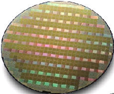
Wafer image courtesy of Xilinx Corporation. Unauthorized use not permitted.
Copyright © 2003-2009 by Savant Company Inc. All rights reserved.
|


 Dr. Thanh
Tran, Senior Member Technical Staff,
Dr. Thanh
Tran, Senior Member Technical Staff,
 Peter
Lee, President & CEO, Aplus Flash Technology
Peter
Lee, President & CEO, Aplus Flash Technology
 Ken Potts,
Sr. Product Marketing Director,
Ken Potts,
Sr. Product Marketing Director, 

 Robert
Madge, Director, Technology Marketing, LSI Logic Corporation
Robert
Madge, Director, Technology Marketing, LSI Logic Corporation  Richard
Gordon, T-Zero Engineering.
Richard
Gordon, T-Zero Engineering.
 D
D Susan
Runowicz-Smith is Marketing Director for Industry Alliances at Cadence
Design Systems, Inc.
Susan
Runowicz-Smith is Marketing Director for Industry Alliances at Cadence
Design Systems, Inc.