|
|
Early Bird Registration Is Now Open! The 14th International System-on-Chip (SoC) Conference, Exhibit & Workshops October 19 & 20, 2016 University of California, Irvine (UCI) - Calit2 |
|
||
|
|
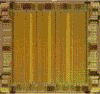
Understanding and Effectively Suppressing the Noise Coupling in Mixed-Signal SoC Applications. By: Dr. Cosmin Iorga.
Description
Introduction:
Semiconductor industry has significantly advanced in the past decades mainly
driven by computing technology, Internet, communication networks, and portable
consumer electronics. Market demands requiring increased functionality and
lower costs have pushed the technology scaling down to sub-micron, deep
sub-micron, and nano-scale dimensions. Technology
scaling has generated the trend to integrate analog and digital blocks on the
same chip, concept referred as mixed-signal integrated circuit, and is heading
towards the goal of implementing a complete system in a single chip, concept
referred as System-on-Chip (SoC). SoCs eliminate the connection between
multiple chips used in previous architectures, thus reducing the number of
output buffers and the cost of packaging and fabrication. Besides
the advantages of integrating more functionality in a single chip, mixed-signal
integrated circuits and SoCs encounter tremendous challenges. These challenges
are generated primarily by the high density of circuits and include coupling
interaction between blocks and interconnects, increased power supply and
substrate noise, and limitations of design and verification tools. Because
mixed-signal integrated circuits and SoCs implement sensitive analog circuits on
the same die with high-speed digital processing circuits, the switching noise
produced by the digital circuits propagates through substrate and power
distribution to the analog circuits, degrading their performance. This problem
aggravates with technology scaling because larger number of transistors and more
functions are implemented in the digital core resulting in more noise injected
into substrate and power distribution circuits. Device scaling increases the
substrate doping concentration to reduce the transistors threshold voltage. As
a consequence, the substrate conductivity increases and provides a lower
resistive path for noise coupling. The device scaling reduces the headroom and
voltage swings in the analog circuits, thus making them more sensitive to the
coupled noise. As transistor sizes are predicted to shrink to smaller and
smaller dimensions, the noise coupling challenges are projected to worsen. To
overcome these challenges, the development of coupling suppression techniques
and circuits less sensitive to noise is essential. This
tutorial builds the skills necessary to efficiently address the noise coupling
challenges in mixed-signal integrated circuits and SoCs. During this tutorial
the attendees develop a thorough understanding of the noise coupling physical
mechanisms at device, chip substrate, interconnects, package, and PCB levels,
and apply this knowledge to understand the applicability and limitations of
various suppression techniques and simulation methodologies. After
completing this tutorial, attendees are expected to be able to identify the
noise coupling mechanisms in a particular design and to choose and implement the
most efficient suppression techniques that match these coupling mechanisms.
Attendees are also expected to be able to select the most effective simulation
tool or set of tools that cover all the noise coupling mechanisms in their
specific chip/package/PCB design, and to create an efficient simulation
methodology that estimates accurately the noise coupling effects after
fabrication. This is an
introductory section that discusses general aspects of noise coupling in
mixed-signal integrated circuits and potential problems that may occur due to
noise coupling. Examples of noise coupling effects on circuits’ performance
are also presented and analyzed. Since in mixed-signal integrated circuits most
of the generated noise depends on the digital activity, in large and complex
chips the noise coupling issues often have an intermittent nature and are hard
to duplicate. The troubleshooting relays on identifying the sequence or
combination of digital vectors that created the problem, which in many cases
depend on the level of testability implemented in the digital cores. To reduce
the chances of having noise coupling issues, designers implement suppression
techniques and estimate the noise coupling effects before fabrication. This
section emphasizes the importance of understanding the noise coupling mechanisms
in the combined chip-package-PCB structure in order to select the right
suppression techniques and simulation methodologies. This
section analyzes the noise generation, propagation, and reception at the
physical structure levels of devices, chips, packages, and printed circuit
boards. The development of equivalent circuits modeling the noise coupling
mechanisms is presented. It is also emphasized that noise couples through both
the common substrate and the power distribution. The architecture of the power
distribution on chip, package, and PCB, and the choice of values and types of
decoupling capacitors have a major impact on noise generation and propagation.
Power distribution resonance and noise generation dependence on the frequency
characteristics of the power distribution impedance is analyzed. Emphasis is
placed on building and improving analysis skills and methodologies so that
attendees can apply the knowledge and techniques learned here to existing and
future devices and technologies. This
section presents and analyzes various noise coupling suppression techniques.
Methods of reducing the noise generation, propagation, and reception are
analyzed with relation to the physical structures of devices, chip substrate,
package, and PCB, discussing the advantages, disadvantages, and limitations of
each method. Traditional guard rings and shields reduce the noise coupling but
do not completely eliminate it. It is illustrated how, in some cases, guard
rings and shields can actually inject additional noise into the protected
regions. To avoid this, the understanding of noise coupling and suppression
mechanisms is essential. It is also discussed the suppression by properly
designing the power distribution at the system, board, package, and chip
levels. The analysis results suggest that the choice and efficiency of
suppression techniques depend directly on the specific noise coupling mechanisms
of each individual case. To overcome the limitations of traditional suppression
techniques, additional circuit level noise cancellation methodologies and
implementation examples are presented and analyzed. This section covers the simulation of noise coupling in integrated circuits. The selection choice and use of conventional methods and tools are analyzed, focusing on the advantages and limitations specific to both post-layout and pre-layout stages of the design flow. It is highlighted the importance of understanding the noise coupling mechanisms before choosing a simulation tool or set of tools. Designers need to make sure the tools used cover all the noise coupling mechanisms in each particular chip-package-PCB structure before trusting the simulation results. Since some decisions that affect noise coupling are typically taken in early stages of the design flow, it is desirable to be able to estimate the noise coupling during the architectural definition of the project. Since most of the existing tools do not offer a practical approach to noise coupling simulation in early stages, this section presents a modeling methodology based only on information typically available in the architectural definition stages of projects. The model is constructed based on the physical structure of devices, technology parameters available in the design guide, and statistical data from typical practices or previous designs. An example showing the model construction and correlation with measurements on a test chip are also presented.
To register for this Workshop, click here: NoiseCoupling Workshop Registration.
Back to Workshops & Tutorials Page
Copyright © 2003-2009 by Savant Company Inc. All worldwide rights reserved.
|
|
|