|
| |
|
Keynotes
15th International System-on-Chip
(SoC)
Conference, Exhibit & Workshops
The Theme for This
Year’s Conference Is “Secure and Intelligence Silicon Systems for
Emerging Applications."
|
|
|
To present and/or exhibit at this
highly-targeted International System-on-Chip (SoC) Conference, please contact:
949-981-1837 or SoC.Conf.Update@Gmail.com |
|
a
|
a
Click Here To
Download The UCI Campus Map
Directions &
Parking for Calit2 Building at the University of California, Irvine (UCI)
a
Platinum Sponsors
a
| |
|
|
|
|
|
|
|
Schedule & Program Summary
|
|
|
|
|
SoC Conference Day 1 |
Wednesday, October 19, 2016
UCI - Calit2 Building |
8:30 am - 6:00 pm |
|
|
|
SoC Conference Day 2 |
Thursday, October 20, 2016
UCI - Calit2 Building |
8:30 am - 6:00 pm |
|
|
|
SoC Tabletop Exhibit &
Reception |
Wednesday, October 19, 2016
UCI - Calit2 Building |
2:00 pm - 7:00 pm |
|
| |
|
|
|
|
a
|
|
Microsemi
Keynote

|
 Jim
Aralis, Chief Technology Officer (CTO), and Vice President of R&D. Jim
Aralis, Chief Technology Officer (CTO), and Vice President of R&D.
“What does a SoC look like
in 2025? Who, what and Why”
Abstract: The talk will
focus on changes in technology, applications, and economics of the SoC
ecosystem, and what it will likely mean for the realization of these devices
in the next decade. It will examine the way process technology, packaging
technology, design abstraction, and other such factors of true
differentiation will push these core devices. These observations are
intended to provide insights into where to position your company and career
for the coming decade.
Bio: Jim Aralis has served as
chief technology officer and vice president of R&D for Microsemi since
January 2007. He has more than 30 years experience in developing custom
analog device and process technologies, analog and mixed-signal ICs and
systems, and CAD systems. Jim played a key role in transitioning Microsemi to a virtually fabless
model, supporting multiple process technologies including, high voltage and
high power BCD/CMOS, high power high integration CMOS, GaAs, SiGe, IPD, RF
CMOS SoI, GaN, SiC, and several high-density packaging technologies.
From 2000 to 2007, Jim established and served as senior design director of
Maxim Integrated Product’s engineering center in Irvine, Calif. Before that,
he spent 7 years with Texas Instruments/ Silicon Systems as mixed-signal
design head and senior principal engineer. Additional experience includes 11
years with Hughes Aircraft Company in positions of increasing responsibility
including senior scientist. Jim earned a bachelor of science degree in
Math Applied Science and Physics and a master of science in electrical
engineering from UCLA. He holds 9 patents for circuit and system design.
|
|
|
|
IBM
 |
 Dr.
Daniel Worledge, Distinguished Research Staff Member, Senior Manager,
MRAM. Dr.
Daniel Worledge, Distinguished Research Staff Member, Senior Manager,
MRAM.
"Spin Torque MRAM."
Abstract: Spin-Transfer-Torque Magnetic Random Access Memory (MRAM)
possesses a unique combination of high speed, high endurance,
non-volatility, and small cell size. Among the emerging new memory
technologies, including phase change memory, resistive random access memory,
and conductive bridging random access memory, Spin Torque MRAM is the only
candidate with the potential for unlimited endurance, since no atoms are
moved during writing. This makes it the only potential candidate for use as
a non-volatile working memory. Write current largely determines the cost of
Spin Torque MRAM, since the transistor and hence cell area must be sized
large enough to source the write current. This talk will give a brief
overview of Spin Torque MRAM, including potential applications and materials
challenges. I will then review the discovery of interface perpendicular
anisotropy in the Ta|CoFeB|MgO system at IBM and the subsequent
perpendicular magnetic tunnel junctions which were developed using it,
including demonstration of reliable, high speed spin-torque writing, and
results on scaling down to 20 nm. Recent experimental results showing low
switching current with 10 ns pulses and theoretical predictions for further
lowering the switching current will also be shown.
Bio: Dr.Daniel C. Worledge IBM Research Division, Almaden Research Center
Dr. Worledge received a BA with a double major in Physics and Applied
Mathematics from UC Berkeley in 1995. He then received a PhD in Applied
Physics from Stanford University in 2000, with a thesis on spin-polarized
tunneling in oxide ferromagnets. After joining the Physical Sciences
Department at the IBM T. J. Watson Research Center as a Post-doc in 2000, he
became a Research Staff Member in 2001, developing fast turn-around
measurement methods for magnetic tunnel junctions, including
Current-in-Plane Tunneling. In 2003, Dr. Worledge became the manager of the
MRAM Materials and Devices group, and in 2013 he became Senior Manager of
MRAM. He has worked on developing Toggle and then Spin Torque MRAM,
including developing new perpendicular magnetic materials. His current
research interests include magnetic devices and their behavior at small
dimensions, and new magnetic devices for logic applications.
|
|
|
|
University of California,
Los Angeles.
Keynote

|
 Dr.
Subramanian S. Iyer, Distinguished Chancellor's Professor Dr.
Subramanian S. Iyer, Distinguished Chancellor's Professor
Charles P. Reames Endowed Chair, Electrical Engineering Department, Henry
Samueli School of Engineering and Applied Science, UCLA.
"A Different
Approach to SoCs"
Abstract: Moore’s law
has so far relied on the aggressive scaling of CMOS silicon minimum features
of over 1000X for over four decades, and recently, on the adoption of
innovative features, such as Cu interconnects, low- dielectrics for
interconnects, strained channels, and high- materials for gate dielectrics,
resulting in a better power performance, cost per function, and density
every generation. This has spawned a vibrant system-on-chip (SoC) approach,
where progressively more function has been integrated on a single die. The
integration of multiple dies on packages and boards has, however, scaled
only modestly by a factor of three to five times. However, as SoC’s have
become more complex and bigger, the NRE and time to market have both
ballooned out of control leading to ever increasing consolidation. In this
presentation, we show that with the apparent slowing down of semiconductor
scaling and the advent of the Internet of Things, there is a focus on
heterogeneous integration and system-level scaling. Packaging is undergoing
a transformation that focuses on overall system performance and cost rather
than on individual components. We propose ways in which this transformation
can evolve to provide a significant value at the system level while
providing a significantly lower barrier to entry compared with a chip-based
SoC approach that is currently used. This transformation is already under
way with 3-D stacking of dies and will evolve to make heterogeneous
integration the backbone of a new SoC methodology.
Bio: Subramanian S. Iyer (Subu)
is Distinguished Chancellor’s Professor and holds the Charles P. Reames
Endowed Chair in the Electrical Engineering Department at the University of
California at Los Angeles and Director of the Center for Heterogeneous
Integration and Performance Scaling (CHIPS). He obtained his B.Tech. from
IIT-Bombay, and Ph.D. from UCLA and joined the IBM T.J. Watson Research
Center at Yorktown heights, NY and later moved to the IBM systems and
Technology Group at Hopewell Junction, NY where he was appointed IBM Fellow
and was till recently Director of the Systems Scaling Technology Department.
His key technical contributions have been the development of the world’s
first SiGe base HBT, Salicide, electrical Fuses, embedded DRAM and 45nm
technology used at IBM and IBM’s development partners to make the first
generation smartphone devices. He also was among the first to commercialize
bonded SOI for CMOS applications through a start-up called SiBond LLC. He
has published over 300 papers and holds over 70 patents. His current
technical interests and work lie in the area of advanced packaging and
three-dimensional integration for system-level scaling and new integration
and computing paradigms as well as the long-term semiconductor and packaging
roadmap for logic, memory and other devices including hardware security and
supply-chain integrity. He has received several outstanding technical
achievements and corporate awards at IBM. He is an IEEE Fellow and a
Distinguished Lecturer of the IEEE EDS as well as its treasurer. He is a
Distinguished Alumnus of IIT Bombay and received the IEEE Daniel Noble Medal
for emerging technologies in 2012. He also studies Sanskrit in his spare
time.
|
|
|
|
Shanghai Institute of
Microsystem and Information Technologies
Keynote
 |
 Professor
Tian Tong, Shanghai Institute of Microsystem and Information Technologies. Professor
Tian Tong, Shanghai Institute of Microsystem and Information Technologies.
"Challenges to Technical
Issues of SiCMOS mmWave SoC Implementation."
Abstract:
Integrating an entire system on a single chip has been a
dream since the earliest days when CMOS IC technologies invented. However,
limited by practical technologies, during the most of the past years SoC
referred to a fully digital system chip. Therefore most SOC researches were
focused on how to implement a huge scale digital system, such as the rule
for high density layout, heat sunk, testable design, clock delay control and
so on. However, with the feature length of SiCMOS process achieving 90nm and
below, it becomes possible for an RF system, and even an mmWave system, to
be integrated into an SOC to construct ‘really’ full-function communication
systems or other electronic systems. This raises many new problems to SOC
research, since the design concerns on analog/RF/mmWave partition are
sensitivity, noise, attenuation and etc which are much different from the
design concerns on digital partition. Moreover, implemented on the same
chip, the two partitions (digital partition and mmWave partition) will
interfere with each other due to the characteristics of the CMOS process.
In the presentation , four sections are to be presented, which are:
1. mmWave SOC, possibility and feasibility. In this section,
the technologies supporting mmWave SOCs are discussed to demonstrate the
possibility of mmWave system implementation. Meanwhile, the advantages of
CMOS SOC solutions for mmWave systems are discussed from technical and
market points of view.
2. Interference between each other: Substrate coupling issue
and an engineering solution. Due to the special PN junction isolation, there
is in fact a path with which all components are connected together. The path
presents a good noise ( or harmonics) channel from the digital partition to
the mmWave partition as well as between noise sources in components. In most
cases, a guardring and/or an isolation gap are chosen as the solution. To
avoid wasting wafer area, and to keep the noise or substrate harmonic level
under control dynamically, an active method is presented. To validate the
method, the harmonic characteristics of digital partitions will be analyzed
and summarized.
3. Low resistance substrate issues for SiCMOS mmWave SOC and
a possible solution. Undoubtedly, SiCMOS low resistance substrate
induces the most issues into SiCMOS mmWave SOC implementation. Compared to
III-V or SOI technologies, CMOS substrates will present a higher noise
floor, noise coupling, devices performance degradation and propagation
attenuation. This presentation will try to analyze the issues and presents
amounts of measurements to systematically discuss the method to improve the
performance of devices and mmWave systems on chip.
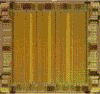
4. A brief introduction of our mmWave SOC design of a single
chip CMOS Radar. Based on fundamental SOC researches, a single chip 35
GHz FMCW radar was designed and implemented in standard CMOS 65nm, which
presents a 1.4GHz FMCW bandwidth, 120mW power consumption, and more than
30dB receiving gain. The principle integrated on-chip blocks include 35GHz
VCO, FMCW generator, Mixer, LNA, on-chip PA, online calibration, SPI control
port, power distribution and management, and IF amplifier and filters, as
well as chip protection. The SOC chip presents users IQ- IF outputs, and a
control port. Users do not need to handle any mmWave signal.
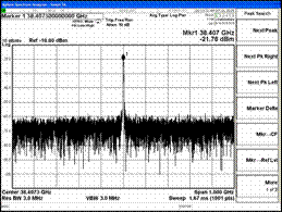
The 35 GHz signal generated on
chip.
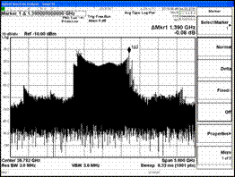
The FMCW signal generated on Chip
with 1.4GHz Bandwidth
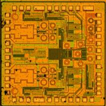
The microphoto of the SOC Die.
Bio:
Professor Tian Tong, obtained his bachelor’ s degree from
microelectronics division of Huazhong University of science and technology
in 1990, master’s degree from circuit and system division of Xi’an
University of electronic science in 1995 and Ph.D degree with the best honor
of TCL from microelectronics division of Xi’an Jiaotong University in 1998 ,
respectively. He took positions of post doc at National key lab of Radar
signal processing in 1998-2000 and Nanyang technological University,
Singapore in 2000-2001. Since 2001 he was with the Institute of
Microeletronics, Singapore as a senior engineer and a senior research
scientist, and was elected as the member of technical council and the member
of invention council. He won the best research Prize of the Institute of
Microeletronics, Singapore for 2003-2004. From August 2004 he held a
position of Associate Professor in Aalborg University, Danmark. And since
March, 2010 he is with Shanghai institute of Microsystems and information
technology as a Professor,and
holds positions of adjunct professor in a few Chinese famous Universities in
the meanwhile. He is associate editor of IEEE transaction on Circuit and
system II. His research area covers analog/RF IC and system; Millimeter wave
IC and system; RF system for Human body implant and human body assistance |
|
|
|
|
|
|
* * * * * * *
Back To The Main SoC
Conference Page
Copyright © 2003-2016 by Savant Company Inc. All
Worldwide Rights Reserved.
| |
|