|
| |
|
If you
have any questions or need more information, please contact:
SoC@SavantCompany.com
or
(714) 532-2461 ― Thank
you!
|
|
a
|
Directions &
Parking for Calit2 Building at the University of California, Irvine (UCI)
For questions regarding the SoC Conference
Keynotes, Presentations, and Panelists opportunities, as well as
Sponsorship & Tabletop Exhibit opportunities, please contact:
SoC@SoCconference.com or
(714) 532-2461
|
|
Microsemi
Keynote

|
 Mathieu
Sureau, Director of Engineering for Analog Mixed Signal, Microsemi
Corporation. Mathieu
Sureau, Director of Engineering for Analog Mixed Signal, Microsemi
Corporation.
Keynote: "Down
the Technology Curve? Not so Fast"
Abstract: Semiconductor companies building SoCs face the same challenge
when designing their next generation device. How to meet the increasing
performance requirements of the diverse market segments they target, achieve
further cost efficiencies and increase value for themselves and their
customers? In most cases, this translates into running down the technology
curve. However, recent studies have shown that these cost savings are
not necessarily realized when going from one technology node to the next.
Even then, heavy and long development cycles, higher voltage requirements
for analog, reliability of technology as well as IP availability constitute
barriers to the latest technology adoption for some applications. Leveraging
one or more established technologies with process extensions in an SoC or in
a Multi-Chip-Module optimizing system partitioning are effective ways to
mitigate these concerns.
Bio: Mathieu Sureau is the
Director of Engineering for Analog Mixed Signal at Microsemi Corporation.
Mathieu has more than 15 years semiconductor experience and oversees the
design and development of Analog and Analog Mixed Signal Semiconductors
serving several markets. These products range from pure analog to
mixed-signal integrated circuits to complete system solutions in a package
on technologies ranging from low voltage CMOS to high voltage, high power,
high integration BCD/CMOS, SOI and DI processes. Mathieu manages the design
and development of High-Reliability Semiconductors used in Defense,
Aerospace, and extreme environment industrial applications including
down-hole drilling. He also oversees the development of
microcontroller-based sensor interface ICs for a variety of
industrial/commercial/automotive applications. More recently, Mathieu’s
management responsibilities have expanded to the development of power
management solutions for commercial storage applications, along with
integrated solutions for light-emitting backlit panels. Mathieu holds a
Masters of Science in Electrical Engineering from ENSEEIHT, Toulouse,
France. He also holds an MBA with concentration in Finance from Santa Clara
University.
 Jim
Aralis, Chief Technology Officer (CTO), and Vice President of R&D. Jim
Aralis, Chief Technology Officer (CTO), and Vice President of R&D.
Abstract: This
presentation will outline the new process, processor, and packaging
technologies that are enabling the expansion of mixed-signal SoC product
development efforts. Subjects that will be covered include the optimization
of design methodologies, mode partitioning, and process selection to
maximize cost-savings, performance, and time-to-market. The presenter will
also discuss how expertise in analog processing, signal conditioning,
precision timing, and high speed wired and wireless communications design
remain critical for designing differentiated products in an expanding and
evolving digital environment.
Bio: Jim Aralis has served as
chief technology officer and vice president of R&D for Microsemi since
January 2007. He has more than 30 years experience in developing custom
analog device and process technologies, analog and mixed-signal ICs and
systems, and CAD systems. Jim played a key role in transitioning Microsemi to a virtually fabless
model, supporting multiple process technologies including, high voltage and
high power BCD/CMOS, high power high integration CMOS, GaAs, SiGe, IPD, RF
CMOS SoI, GaN, SiC, and several high-density packaging technologies.
From 2000 to 2007, Jim established and served as senior design director of
Maxim Integrated Product’s engineering center in Irvine, Calif. Before that,
he spent 7 years with Texas Instruments/ Silicon Systems as mixed-signal
design head and senior principal engineer. Additional experience includes 11
years with Hughes Aircraft Company in positions of increasing responsibility
including senior scientist. Jim earned a bachelor of science degree in
Math Applied Science and Physics and a master of science in electrical
engineering from UCLA. He holds 9 patents for circuit and system design.
|
|
|
|
Skyworks Solutions, Inc.
Keynote

|

James P. Young Vice
President, Advanced Development, Skyworks Solutions, Inc.
Keynote: "Mobile Front End Module The Battle Between SIP & SoC."
Bio: James P. Young is vice
president of advanced development at Skyworks Solutions, Inc. where he is
responsible for mobile handset power amplifier and front end module design.
His expertise includes power amplifier and RFIC circuit and system design in
CMOS, SOI, BiCMOS, bipolar, and GaAs technologies. James holds 18 patents,
has authored or co-authored over 22 papers, and taught several short courses
mainly on RFIC design. He holds a bachelor’s of science in electrical
engineering from Rose-Hulman Institute of Technology in Terra Haute,
Indiana.

Dr. Peter L. Gammel, Chief
Technology Officer (CTO), Skyworks Solutions, Inc.
Abstract: Ubiquitous
demand for mobile platforms with extended talk times and high-speed data is
creating an unprecedented level of analog and RF complexity. As the wireless
market transitions from 3G to 4G standards such as LTE and LTE-A, front-end
architectural challenges are being compounded by demanding coexistence,
shielding and harmonic requirements above and beyond the traditional
constraints of power efficiency, size and cost. Front-end solutions will
soon have to support up to 50 frequency bands and 100 carrier aggregation
combinations. Next-generation products will also support LTE in WiFi, GPS,
Bluetooth®, Mobile TV, NFC and other non-cellular services.
While higher peak to average modulations are driving significant innovation
in power added efficiency in the basic transistor characteristics, and
system level approaches including DPD, APT and envelope tracking when
combined can reduce power consumption by up to 30 percent, GaAs HBT
technology and roadmap maintains a 10 percent efficiency advantage over SOI
and CMOS. Another critical technology for system level efficiency is antenna
tuning, where switches can be applied for both on-antenna aperture tuning as
well as the antenna-feed impedance tuning.
Both system-in-package and system-on-chip approaches are being pursued to
integrate all of the RF and analog content between the transceiver and
antenna, including multiband power amplifiers, high throw switches,
filtering, duplexing and controls. System-in-package solutions such as
Skyworks’ SkyOne™ family of products use multiple technologies to optimize
the performance, size and cost of each functional block and provide a fully
shielded and packaged solution to address co-existence and interference as
the size of the RF board continues to shrink.
Bio: Peter L. Gammel,
53, is chief technology officer for Skyworks Solutions, Inc. He joined the
company in June 2011 as part of Skyworks' acquisition of SiGe Semiconductor.
At SiGe, he served as chief technology officer and vice president of
engineering. Prior to this, he was vice president of engineering at
Renaissance Wireless and chief technology officer at AdvanceNanotech and for
Agere Systems' Analog Products Business. He was also a distinguished member
of technical staff at Alcatel-Lucent Bell Labs. Gammel received a
bachelor's of science in physics and mathematics from Massachusetts
Institute of Technology and a Ph.D. in physics from Cornell University.
|
|
|
|
Tohoku University
Japan
Keynote

|

Dr. Takahiro Hanyu, New
Paradigm VLSI System Research Group, Laboratory for Brainware Systems,
Research Institute of Electrical Communication- Tohoku University.
Keynote: "MTJ/MOS-Hybrid Nonvolatile Logic-in-Memory Architecture Towards
Ultra-Low-Power LSIs"
Abstract: In the
Internet of Everything (IoE) era, it is strongly necessary to achieve
ultra-low-power computer architecture, while still keeping high-performance
computer power, because computer terminals distributed into everything must
be operated under the limitation of energy harvested from natural resources.
However, in the present CMOS-only-based VLSI, communication bottleneck
between memory and logic modules inside a VLSI chip, as well as increasing
standby power dissipation and device-characteristic variation effect, has
increasingly become a serious problem. One approach to solving the above
problem is to use "nonvolatile logic-in-memory" architecture, where
nonvolatile storage elements are distributed over a logic-circuit plane. One
of the nonvolatile storage devices, magnetic tunnel junction (MTJ), has a
good compatibility to the present CMOS-based VLSI chips, so that it is
expected to realize both ultra-low-power and reduced interconnection delay
because of great reduction of global interconnection counts and volatile
storage-element counts. In this sense, nonvolatile logic-in-memory
architecture is implemented using magnetic tunnel junction (MTJ) devices in
combination with MOS transistors. In this presentation, new logic-VLSI
architecture called “nonvolatile logic-in-memory architecture (NV-LIM)” is
introduced as a promising candidate to solve the above emerging problems. As
concrete design examples of the proposed nonvolatile logic-in-memory
circuitry, I demonstrate a nonvolatile Ternary Content-Addressable Memory
[1-2], an instant power-ON/OFF nonvolatile Field Programmable Gate Array
[3-5], and so on [6].
I am also focusing on a post-process variation-resilient logic-circuit
design using MTJ devices [7-8].
Bio: Takahiro Hanyu
received the B.E., M.E. and D.E. degrees in Electronic Engineering from
Tohoku University, Sendai, Japan, in 1984, 1986 and 1989, respectively. He
is currently a Professor in the Research Institute of Electrical
Communication (RIEC), Tohoku University. His general research interests
include nonvolatile logic circuits and their applications to ultra-low-power
and/or PVT-variation-free VLSI processors, and multiple-valued current-mode
circuit and its application to power-aware asynchronous Network-on-Chip
systems. He received the Sakai Memorial Award from the Information
Processing Society of Japan in 2000, the Judge's Special Award at the 9th
LSI Design of the Year from the Semiconductor Industry News of Japan in
2002, the Special Feature Award at the University LSI Design Contest from
ASP-DAC in 2007, the APEX Paper Award of Japan Society of Applied Physics in
2009, the Excellent Paper Award of IEICE, Japan, in 2010, Ichikawa Academic
Award in 2010, the Best Paper Award of IEEE ISVLSI 2010, and the Paper Award
of SSDM 2012. Dr. Hanyu is a Senior Member of the IEEE.
|
|
|
|
CEA-LETI, France
Keynote


|

Hughes Metras, VP,
Strategic Partnerships., CEA-LETI, France.
Keynote: "3D VLSI a disruptive approach for further scaling."
Abstract: COOLCUBE™, a
semiconductor process concept developed by CEA-LETI, aims at stacking
transistors on top of each other sequentially in the same process flow for
3D-VLSI purpose. It has been introduced as an alternative to the traditional
scaling paradigm where technology challenges and costs of new node
development become difficult to justify economically. COOLCUBE™ will enable
an increased density of transistors without requiring the downscaling of
their individual features. It could also provide a gain in performance by
reducing the metal wiring delay, thanks to direct contact between transistor
levels. The concept consists in sequentially processing a
Low-Temperature-Budget MOS transistor (“COOL”) layer on top (“CUBE”) of a
first bottom MOS transistor layer with a lithographic alignment precision
between the layers. Metal lines are positioned between both layers to allow
design of connections between both transistor levels. Inter-metal levels are
encapsulated by an oxide layer, to add the substrate for the top transistor
layer by molecular bonding, while using a planarization process.
The presentation will detail the principles of this new approach with a
highlight on the key technological challenges that have to be tackled in the
coming years to enable large scale manufacturability. These mainly include
the development of a low temperature process flow for the top layer
transistors to avoid any impact on the performances and stability of the
bottom layer transistors while providing enough performance to the top layer
devices themselves. The presentation will also mention what has to be
develop to implement an adequate design flow including a predictive Design
kit based on SPICE model and relevant Model Cards based on data coming from
real device measurements. An evaluation of potential advantages for COOLCUBE™
devices such as FPGAs and other SOC will be described and future
applications will be proposed including 3D-VLSI Gate Option to gain IC
performance through reduced wire length and 3D- VLSI TR option performance
at the transistor level via independent transistor optimization (3-5 based
NFET with Ge base pFET for instance).
Bio: Hughes Metras is VP
in charge of Strategic Partnerships in North America for CEA-LETI, a major
European R&D lab with 200 and 300 mm facilities in Grenoble France. He is
also a visiting staff member at Caltech in the framework of the Alliance for
Nanosystems VLSI. Previously, Hughes was VP Marketing and Sales, in charge
of business development and strategic planning. He coordinated Leti's sales
and marketing teams in the field of semiconductors (advanced CMOS,
Heterogenous Integration), imaging and photonics, biomedical technologies as
well as telecommunications. He was involved in major French initiatives with
key industrial players for the emergence of new programs in microelectronics
addressing new societal challenges such as power conversion for industrial,
automotive and PV applications and low power electronics. He has also been
involved in the European technology platform EPOSS (smart system
integration) where he coordinated the working group on key technologies and
was a member of the executive committee. Mr. Metras is based in Pasadena,
California.
|
|
|
|
|
|
|
|
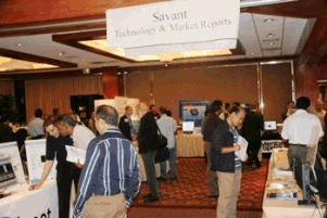
Selected
Technology
&
Media
Sponsors |
|
* * * * * * *
Back To The Main SoC
Conference Page
Copyright © 2003-2014 by Savant Company Inc. All
Worldwide Rights Reserved.
Wafer images courtesy of Intel Corporation, Micron Technologies & Altera Corporation.
| |
|