|
| |
|
SoC Conference Presenters'
Bios & Abstracts
12th International System-on-Chip
(SoC)
Conference, Exhibit & Workshops
The Theme for This Year’s
Conference Is “Innovative SoCs, Empowering the Communications Market.”
|
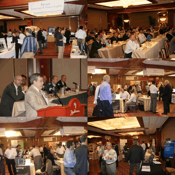 |
|
If you
have any questions or need more information, please contact:
SoC@SavantCompany.com
or
949-981-1837 ― Thank
you!
a
|
|
|
Click Here To
Download The UCI Campus Map
Directions &
Parking for Calit2 Building at the University of California, Irvine (UCI)
|
|
|
|
|
|
|
|
Day
One Wednesday October 22, 2014
SoC Conference Program Agenda* |
|
|
|
Savant
Company Inc.
 |
 Farhad
Mafie, SoC Conference Chairman,
IEEE OC SSCS & OCEN Chairs. Farhad
Mafie, SoC Conference Chairman,
IEEE OC SSCS & OCEN Chairs.
Welcome and Opening Remarks, Technology/Market Trends.
Farhad Mafie is SoC Conference
Chairman. He has over
20 years of experience in semiconductor and computer businesses and more
than 10 years of university-level teaching experience. He is the former Vice
President of Marketing and Engineering at Toshiba Semiconductor. He has also
worked in strategic marketing, project and design engineering at Lucent
Technologies, Unisys, and MSI Data. Farhad has a Master of Science and a
Bachelor of Science degree in Electronic Engineering from California State
University, Fullerton. He is an author and a translator, and his articles
have been published in a variety of journals and Web-based magazines on
technology and political affairs. In 2003, he published the biography of
Iranian poet and Nobel nominee who lived in exile, Nader Naderpour
(1929-2000), Iranian Poet, Thinker, Patriot. Farhad is also Editor-in-Chief
for the CRC Press SoC Design and Technologies Book Series, which includes
(1) Low-Power NoC for High-Performance SoC Design and (2) Design of
Cost-Efficient Interconnect Processing Units. Farhad is an active member of
IEEE, and he is the chair of IEEE Orange County Solid-State Circuits Society
(SSCS), as well as IEEE Orange County Entrepreneurs' Network (OCEN). He is
also a member of two UCI Advisory Committees: Communication System
Engineering and Embedded System Engineering Certificate Programs.
|
|
|
|
|
|
|
|
|
UCLA
 |
 Yunshan
Jiang, Peter DeVore, Jacky Chan, Bahram Jalali, UCLA Yunshan
Jiang, Peter DeVore, Jacky Chan, Bahram Jalali, UCLA
“Optical Computing with Silicon Photonics."
Abstract: With proliferation
of big data and the ever increasing power dissipation of electronic data
processors, there is renewed interest in the use of optics in computing [ONR
MURI]. In contrast to the optical computing efforts of the past, it is now
recognized that an all-optical computer may not be the most prudent goal.
Instead, a hybrid approach where optics is selectively used to alleviate
bottlenecks and assist electronic processors is a more fruitful pursuit. In
this paper, we investigate the prospects of silicon photonics for
implementing analog optical computational functions. To focus the discussion
and to give two concrete examples: (1) the fundamental mathematical
operation of computing the nth-power of a real number, and (2) performing
Fourier transform of ultrafast signals. The first operation can be achieve
through analog operations of logarithm, amplification/attenuation, and
exponential functions. The second operation can be performed using the
Time-Stretch Dispersive Fourier Transform (TS-DFT). We present ways to
perform these operations using silicon’s optical properties and discuss
their limitations.
Starting at the 90nm
node, to meet the performance, power and density needed to stay on track
with Moore’s Law, the process complexity of integrated circuit fabrication
has steadily increased. The adoption of new materials, new process/tools and
lately new device architecture such as FDSOI, Multi-Gate device architecture
such as FinFET, NanoWire has resulted in a tremendous increase in wafer
processing cost and design cost to extend the life of the bulk MOSFET for
SoC application. Alternate solution using SmartcutTM to transfer high
mobility material on thin BOX for back bias and/or forming the local
strained SiGe/Ge for enhancing performance, better performance/power
trade-off and cost effective solution will be reviewed.
Bio: TBA.
|
|
|
|
WiSpry,
Inc.
 |
 Jeffrey
L. Hilbert, CEO & Founder, WiSpry, Inc. Jeffrey
L. Hilbert, CEO & Founder, WiSpry, Inc.
“Widely Tunable MMMB Wireless Front-Ends Using RF-CMOS MEMS."
Abstract: Continued rapid growth of LTE has intensified requirements for
disruptive technology to implement next generation radio hardware that
provides global connectivity and meets the stringent RF requirements of LTE
Advanced architectures including MIMO antenna systems and carrier
aggregation. RF-MEMS has emerged as the leading candidate to implement
software programmable, tunable, RF hardware by providing near zero loss,
ultra-linear RF device and circuit performance. Recent progress in such
tunable components has demonstrated numerous benefits including the costs
and scalability required for success in the mobile market.
This talk will review RF-MEMS in consumer mobile applications. A
state-of-the-art, tunable, MMMB, RF front-end implemented with digital
RF-CMOS MEMS, which provides global LTE-A connectivity will be discussed.
Bio: Jeffrey L. Hilbert is the CEO and founder of WiSpry, Inc., a fabless
semiconductor company utilizing CMOS-integrated radio frequency
micro-electro-mechanical systems (RF-MEMS) technology to develop tunable RF
products for the cellular communications and wireless consumer electronics
markets. WiSpry defined and pioneered the Tunable RF market segment that is
now projected to grow to over $1.7B in annual revenues by 2017. Jeff has
over 37 years of executive management and technical experience in a number
of leading semiconductor and MEMS companies including LSI Logic, Compass
Design Automation, AMCC, Motorola, Harris and Coventor. Early in his career,
Jeff did pioneering work in CMOS technology, and in IC design tools leading
to today’s design automation tools that are supplied by companies such as
Cadence. An experienced entrepreneur, Jeff has raised over $120M in
financing to fund two consecutive start-up semiconductor companies over the
past fifteen years. Jeff also has board of directors and advisory board
experience in the commercial, government, and academic arenas. Mr. Hilbert
holds a BS in Chemical Engineering from the University of Florida, an MS in
Computer Science from Florida Institute of Technology, and has done course
work towards a PhD in Computer Engineering from North Carolina State
University.
|
|
|
|
EPFL
(Swiss Federal Institute of
Technology), Lausanne, Switzerland

|
 Dr.
Pierre-Emmanuel Gaillardon, EPFL (Swiss Federal Institute of Technology),
Lausanne, Switzerland. Dr.
Pierre-Emmanuel Gaillardon, EPFL (Swiss Federal Institute of Technology),
Lausanne, Switzerland.
"Towards the Use of Functionality-Enhanced Devices: A Transversal Design
Approach."
Abstract: Exploiting unconventional physical properties, several nanodevices
showed an alternative to Moore’s Law by the increase of their functionality
rather than the pure scaling. Innovative device behaviors transduce to new
circuit/architecture opportunities. Here, we focus on a novel class of
computation devices that exhibit controllable-polarity property. At advanced
technology nodes, Schottky contacts at channel interfaces are becoming
challenging to avoid. Hence, devices face an ambipolar behavior, i.e., that
the device exhibits n- and p-type characteristics simultaneously. Such a
property is desirable for logic computation. Indeed, it has been recently
demonstrated by EPFL that by constructing independent double-gate structures
on Vertically stacked nanowires FETs (NWFETs), the device polarity can be
electrostatically forced to be either n- or p-type. Controllable-polarity
devices are logical bi-conditional on both gate values and enable a compact
realization of XOR-based logic functions, which are not implementable in
CMOS in a compact form. Hyper regular architectures and new EDA tools are
then needed to leverage the intrinsic properties of controllable-polarity
devices from an application perspective. In this talk, I will cover the
different aspects of the design with controllable-polarity devices ranging
from device fabrication to logic synthesis tools, and I will emphasize on
the work organization and importance for interdisciplinary teams in the
field of emerging technologies
Bio: Pierre-Emmanuel Gaillardon works for EPFL, Lausanne, Switzerland, as a
research associate at the Laboratory of Integrated Systems (LSI). He holds
an Electrical Engineer degree (CPE-Lyon, France, 2008), a M.Sc. degree (INSA
Lyon, France, 2008) and a Ph.D. in Electrical Engineering (University of
Lyon, France, 2011). Previously, he was research assistant at CEA-LETI,
Grenoble, France. The research activities and interests of Dr. Gaillardon
are currently focused on nanoscale devices and their use in digital circuits
and architectures.
|
|
|
|
Arizona State University

|
 Professor
Yu (Kevin) Cao, Arizona State University. Professor
Yu (Kevin) Cao, Arizona State University.
"On-chip Learning with the Cross-point Array of Resistive Memory Cells"
Abstract: Revolutionary
advances are taking place in computational neuroscience, machine learning
and nanoelectronics. The convergence of these disciplines is enabling the
feasibility of new hardware design for on-chip learning, offering
information processing capabilities that can never been achieved by
conventional von Neumann architecture. On the other side, even with
state-of-the-art algorithms and multi-core CPUs/GPUs/FPGAs, solving a
machine learning problem still requires expensive computations, especially
during the training step. In this context, this talk presents an exploratory
design practice with emerging memory devices, parallel circuit architecture,
and sparse coding, in order to achieve >2000X acceleration in image feature
extraction. The design principle is to recognize the properties of learning
algorithms, which involve intensive parallel operations of matrix/vector
multiplication/addition, and to construct appropriate devices and circuits
that realize full parallelism. The proposed architecture consists of an
array of resistive memory cells, and CMOS peripheral circuits for input and
output neurons. Two essential operations, Read and Write, are applied to the
cross-point array. This architecture performs key matrix operations, such as
matrix product and Read/Write of matrix elements, in a fully parallel
fashion. Such parallelism enables high-speed matrix operations, at a speed
that is independent of the matrix dimension. The optimized cross-point array
with peripheral circuitry is benchmarked at the 65nm node. Compared to a
cutting-edge software approach, it achieves >2000 speedup and >106 energy
efficiency improvement, enabling real-time learning in mobile applications.
Bio: Yu (Kevin) Cao received the B.S. degree in physics from Peking
University in 1996. He received the M.A. degree in biophysics and the Ph.D.
degree in electrical engineering from University of California, Berkeley, in
1999 and 2002, respectively. He joined Arizona State University in 2004
where he is now an Associate Professor of Electrical Engineering. He has
published more than 190 articles and two books. His research interests
include physical modeling of nanoscale technologies, design solutions for
variability and reliability, reliable integration of post-silicon devices,
and hardware design for neural computing. Dr. Cao received the 2012 Best
Paper Award at ISVLSI, 2010/2012/2013 Teaching Excellence Award, Schools of
Engineering, ASU, 2009 ACM SIGDA Outstanding New Faculty Award, the 2007
Best Paper Award at ISLPED, the 2006 NSF CAREER Award, the 2006 and 2007 IBM
Faculty Award, the 2004 Best Paper Award at ISQED, and the 2000 Beatrice
Winner Award at ISSCC. He has served on numerous technical program
committees and is a member of the IEEE EDS Compact Modeling Technical
Committee.
|
|
|
|
GLOBALFOUNDRIES
 |
 Srinivas
Nori, Director, SoC Solutions, Advanced Technology Architecture,
GLOBALFOUNDRIES. Srinivas
Nori, Director, SoC Solutions, Advanced Technology Architecture,
GLOBALFOUNDRIES.
"Application Specific SoC Solutions - A Foundry Perspective"
Abstract: This presentation
will highlight how GLOBALFOUNDRIES, as a leading foundry, is offering key
SoC solutions that help address the demanding and varied PPA challenges of
today's complex SoCs for different market segments like wearables/IoT,
mobility, consumer, compute, connect, storage, automotive and industrial.
The SoC solution offerings discussed will cover both the mainstream process
technologies as well as the leading edge deep sub-micron technologies.
Bio:
TBD.
|
|
|
|
Morning Break |
Morning Break |
|
|
|
Microsemi
Keynote

|
 Mathieu
Sureau, Director of Engineering for Analog Mixed Signal, Microsemi
Corporation. Mathieu
Sureau, Director of Engineering for Analog Mixed Signal, Microsemi
Corporation.
Keynote: "Down
the Technology Curve? Not so Fast"
Abstract: Semiconductor companies building SoCs face the same challenge
when designing their next generation device. How to meet the increasing
performance requirements of the diverse market segments they target, achieve
further cost efficiencies and increase value for themselves and their
customers? In most cases, this translates into running down the technology
curve. However, recent studies have shown that these cost savings are
not necessarily realized when going from one technology node to the next.
Even then, heavy and long development cycles, higher voltage requirements
for analog, reliability of technology as well as IP availability constitute
barriers to the latest technology adoption for some applications. Leveraging
one or more established technologies with process extensions in an SoC or in
a Multi-Chip-Module optimizing system partitioning are effective ways to
mitigate these concerns.
Bio: Mathieu Sureau is the
Director of Engineering for Analog Mixed Signal at Microsemi Corporation.
Mathieu has more than 15 years semiconductor experience and oversees the
design and development of Analog and Analog Mixed Signal Semiconductors
serving several markets. These products range from pure analog to
mixed-signal integrated circuits to complete system solutions in a package
on technologies ranging from low voltage CMOS to high voltage, high power,
high integration BCD/CMOS, SOI and DI processes. Mathieu manages the design
and development of High-Reliability Semiconductors used in Defense,
Aerospace, and extreme environment industrial applications including
down-hole drilling. He also oversees the development of
microcontroller-based sensor interface ICs for a variety of
industrial/commercial/automotive applications. More recently, Mathieu’s
management responsibilities have expanded to the development of power
management solutions for commercial storage applications, along with
integrated solutions for light-emitting backlit panels. Mathieu holds a
Masters of Science in Electrical Engineering from ENSEEIHT, Toulouse,
France. He also holds an MBA with concentration in Finance from Santa Clara
University.
 Jim
Aralis, Chief Technology Officer (CTO), and Vice President of R&D. Jim
Aralis, Chief Technology Officer (CTO), and Vice President of R&D.
Abstract: This
presentation will outline the new process, processor, and packaging
technologies that are enabling the expansion of mixed-signal SoC product
development efforts. Subjects that will be covered include the optimization
of design methodologies, mode partitioning, and process selection to
maximize cost-savings, performance, and time-to-market. The presenter will
also discuss how expertise in analog processing, signal conditioning,
precision timing, and high speed wired and wireless communications design
remain critical for designing differentiated products in an expanding and
evolving digital environment.
Bio: Jim Aralis has served as
chief technology officer and vice president of R&D for Microsemi since
January 2007. He has more than 30 years experience in developing custom
analog device and process technologies, analog and mixed-signal ICs and
systems, and CAD systems. Jim played a key role in transitioning Microsemi to a virtually fabless
model, supporting multiple process technologies including, high voltage and
high power BCD/CMOS, high power high integration CMOS, GaAs, SiGe, IPD, RF
CMOS SoI, GaN, SiC, and several high-density packaging technologies.
From 2000 to 2007, Jim established and served as senior design director of
Maxim Integrated Product’s engineering center in Irvine, Calif. Before that,
he spent 7 years with Texas Instruments/ Silicon Systems as mixed-signal
design head and senior principal engineer. Additional experience includes 11
years with Hughes Aircraft Company in positions of increasing responsibility
including senior scientist. Jim earned a bachelor of science degree in
Math Applied Science and Physics and a master of science in electrical
engineering from UCLA. He holds 9 patents for circuit and system design.
|
|
|
|
Lunch |
Lunch |
|
|
|
Skyworks Solutions, Inc.
Keynote

|

James P. Young Vice
President, Advanced Development, Skyworks Solutions, Inc.,
Keynote: "Mobile Front End Module The Battle Between SIP & SoC."
Bio: James P. Young is vice
president of advanced development at Skyworks Solutions, Inc. where he is
responsible for mobile handset power amplifier and front end module design.
His expertise includes power amplifier and RFIC circuit and system design in
CMOS, SOI, BiCMOS, bipolar, and GaAs technologies. James holds 18 patents,
has authored or co-authored over 22 papers, and taught several short courses
mainly on RFIC design. He holds a bachelor’s of science in electrical
engineering from Rose-Hulman Institute of Technology in Terra Haute,
Indiana.

Dr. Peter L. Gammel, Chief
Technology Officer (CTO), Skyworks Solutions, Inc.
Keynote: "Turning Complexity into Breakthrough Simplicity"
Abstract: Ubiquitous
demand for mobile platforms with extended talk times and high-speed data is
creating an unprecedented level of analog and RF complexity. As the wireless
market transitions from 3G to 4G standards such as LTE and LTE-A, front-end
architectural challenges are being compounded by demanding coexistence,
shielding and harmonic requirements above and beyond the traditional
constraints of power efficiency, size and cost. Front-end solutions will
soon have to support up to 50 frequency bands and 100 carrier aggregation
combinations. Next-generation products will also support LTE in WiFi, GPS,
Bluetooth®, Mobile TV, NFC and other non-cellular services.
While higher peak to average modulations are driving significant innovation
in power added efficiency in the basic transistor characteristics, and
system level approaches including DPD, APT and envelope tracking when
combined can reduce power consumption by up to 30 percent, GaAs HBT
technology and roadmap maintains a 10 percent efficiency advantage over SOI
and CMOS. Another critical technology for system level efficiency is antenna
tuning, where switches can be applied for both on-antenna aperture tuning as
well as the antenna-feed impedance tuning.
Both system-in-package and system-on-chip approaches are being pursued to
integrate all of the RF and analog content between the transceiver and
antenna, including multiband power amplifiers, high throw switches,
filtering, duplexing and controls. System-in-package solutions such as
Skyworks’ SkyOne™ family of products use multiple technologies to optimize
the performance, size and cost of each functional block and provide a fully
shielded and packaged solution to address co-existence and interference as
the size of the RF board continues to shrink.
Bio: Peter L. Gammel,
53, is chief technology officer for Skyworks Solutions, Inc. He joined the
company in June 2011 as part of Skyworks' acquisition of SiGe Semiconductor.
At SiGe, he served as chief technology officer and vice president of
engineering. Prior to this, he was vice president of engineering at
Renaissance Wireless and chief technology officer at AdvanceNanotech and for
Agere Systems' Analog Products Business. He was also a distinguished member
of technical staff at Alcatel-Lucent Bell Labs. Gammel received a
bachelor's of science in physics and mathematics from Massachusetts
Institute of Technology and a Ph.D. in physics from Cornell University.
|
|
|
|
IEEE Solid-State Circuits
Distinguished Lecturer, Qualcomm Technologies Inc.

|
 Dr.
Alvin Loke, IEEE Solid-State Circuits Distinguished Lecturer, Qualcomm
Technologies Inc. Dr.
Alvin Loke, IEEE Solid-State Circuits Distinguished Lecturer, Qualcomm
Technologies Inc.
"IC Technology at New Nodes Made Easy!"
Abstract: Despite increasing economic and technical challenges to scale
CMOS, we continue to witness unprecedented performance with fully-depleted
tri-gate devices now well in production. This tutorial seminar offers a
summary of how CMOS device technology has progressed over the past two
decades. We will review MOS device and short-channel fundamentals to
motivate how device architectures in production have evolved to incorporate
elements such as halos and spacers, mechanical strain engineering, high-K
dielectric and metal gate, fully-depleted device architectures and finally,
tri-gate finFETs.
Bio: Alvin Loke received his BASc degree from University of BC, and MS and
PhD degrees from Stanford. His doctoral work focused on copper interconnects
with low-K polymer dielectrics. From 1998 to 2001, he worked on CMOS
technology integration at HP Labs and then at Chartered Semiconductor
Manufacturing as an Agilent assignee. In 2001, he moved to Fort Collins,
Colorado where he designed CMOS PLL circuits for SerDes. From 2006 to 2013,
he was with Advanced Micro Devices where he designed high-speed
electrical/optical link circuits and addressed analog/mixed-signal concerns
for next-generation CMOS. He recently joined Qualcomm where he works on
mobile IO links. Alvin has authored over 40 publications and holds 15 US
patents. He served on the CICC technical program committee, as Guest Editor
of the IEEE Journal of Solid-State Circuits, and as an IEEE Distinguished
Lecturer. He was an active SSCS chapter officer in Fort Collins for 10
years. |
|
|
|
4:25 – 5:25
Panel


"FREE"
|
Panel:
“Emerging
and Innovative SoC Solutions and Technologies for Wearable Applications."
Moderator: Farhad Mafie, SoC Conference Chairman, IEEE OC SSCS &
OCEN Chairs.
Panelists:
1.
Rajesh Shah, CEO, Sibridge Technologies.
2. Mike Noonen, Co-Founder, Silicon Catalyst
3. Francois Pelletier, Product Marketing
Director for Ultra Low Power Radios, Microsemi
4. Linh
Hong, VP Marketing at Kilopass Technology.
5. Matt Kammerait, VP Product, DAQRI.
6. Amir Banifatemi, Managing Partner, K5 Ventures.
This
Panel Is Open To Everyone . . . Register Online for FREE Panel Pass
More
Updates Coming Soon . . .
Several
Opportunities to Win various Prizes During this Panel Discussion . . .
Don't
Miss Out! |
|
|
|
Microsemi

|
 Rajesh
Shah, CEO, Sibridge Technologies. Rajesh
Shah, CEO, Sibridge Technologies.
Panelist.
Bio:Rajesh Shah is a serial entrepreneur with more than 17 years of
experience in engineering and business development of semiconductors. His
strength lies in identifying and unlocking the optimal value for customers
in technology products and services.
Prior to Sibridge, Rajesh Shah started and managed the IP and System
Solutions group for Open- Silicon, one of the fasted growing fabless ASIC
companies in the industry. Previously, Rajesh Shah was CEO of chip start-up
Xpedite Communications (successfully acquired by Multilink Technologies, now
part of Vitesse). Xpedite Communication was the first chip company to
develop an ASIC for 16G Ethernet processing engine with multiple end
applications (Router aggregation, VCAT or VOD). Before Xpedite, Rajesh was a
founding employee of Photuris (acquired by Meriton Networks Inc.), where he
managed 2 ASICs for 10G MPLS switch over DWDM. Rajesh started his career as
an UltraSPARC design engineer at Sun before leading an ASIC at Pipelinks
(acquired by Cisco). Rajesh has a Masters in Electrical Engineering from the
University of Texas at Austin.
|
|
|
|
Microsemi

|
 Francois
Pelletier, Product Marketing Director for Ultra Low Power Radios, Microsemi. Francois
Pelletier, Product Marketing Director for Ultra Low Power Radios, Microsemi.
Panelist.
Bio: Francois Pelletier is Product Line Director of the Medical Product
Group at Microsemi where he oversee the Ultra-low power RF transceiver
product family for the medical devices and applications such as implant
devices. Francois has more than 15 years of experience in the development of
electronic subcomponents for medical applications. He holds a Bachelor
degree in electrical engineering and Diploma in Administration from the
University of Sherbrooke, Canada. |
|
|
|
Silicon Catalyst

|
 Mike
Noonen, Co-Founder, Silicon Catalyst. Mike
Noonen, Co-Founder, Silicon Catalyst.
Panelist.
Bio: Mike Noonen is a co-founder of Silicon Catalyst, the silicon solution
start-up incubator based in Silicon Valley. Silicon Catalyst accelerates
innovation and value creation through an industry coalition providing
support, resources, and mentorship. He is a director of Kilopass, Adapteva
and Ambiq Logic. Noonen was Executive Vice President, Global
Products, Design, Sales, & Marketing at GlobalFoundries. He also served on
the Global Semiconductor Alliance Board of Directors and was Chairman of the
Board of Socle, a design services company acquired by Foxconn.
Noonen has held executive roles at NXP Semiconductors, National
Semiconductor, Cisco Systems and 8x8. He started his career at NCR
Microelectronics as an FAE. He has a BSEE from Colorado State University and
in 2012 was named the College of Engineering Distinguished Alumni. He holds
multiple patents in the areas of Internet telephony and video
communications. |
|
|
|
Kilopass
Technology

|
 Linh
Hong, VP Marketing at Kilopass Technology. Linh
Hong, VP Marketing at Kilopass Technology.
Panelist.
Bio: TBA. |
|
|
|
DAQRI

|
 Matt
Kammerait, VP Product, DAQRI. Matt
Kammerait, VP Product, DAQRI.
Panelist.
Bio: Early in his career, as creator and Product Manager for Quad/Graphics'
Interactive Print Solutions, Matt led the process of integrating mobile with
the printed page. The groups offerings included QR Codes, Image Recognition,
Augmented Reality, Near Field Communications (NFC) and other emerging
technologies. Since that time, Matt has joined Augmented Reality
leader DAQRI to expand and push the bleeding edge of 4D technologies. As VP
of Product, he leads Daqri's Product team and Roadmap across Marketing,
Educational, and Industrial market segments. Daqri provides tools and
technologies that allow anyone to create in and leverage Augmented Reality
and the broader 4D medium, with no development required. Matt’s team is
responsible for setting strategic direction and product strategy for DAQRI’s
software and hardware efforts including DAQRI 4D Studio and the recently
announced DAQRI Smart Helmet. His background includes study in Human Factors
and Behavioral Psychology. |
|
|
|
|
Day TWO Thursday, October 23, 2014
SoC Conference Program Agenda* |
|
|
|
Savant
Company Inc.
 |
 Farhad
Mafie, SoC Conference Chairman,
IEEE OC SSCS & OCEN Chairs. Farhad
Mafie, SoC Conference Chairman,
IEEE OC SSCS & OCEN Chairs.
Bio: Farhad Mafie is SoC Conference
Chairman. He has over
20 years of experience in semiconductor and computer businesses and more
than 10 years of university-level teaching experience. He is the former Vice
President of Marketing and Engineering at Toshiba Semiconductor. He has also
worked in strategic marketing, project and design engineering at Lucent
Technologies, Unisys, and MSI Data. Farhad has a Master of Science and a
Bachelor of Science degree in Electronic Engineering from California State
University, Fullerton. He is an author and a translator, and his articles
have been published in a variety of journals and Web-based magazines on
technology and political affairs. In 2003, he published the biography of
Iranian poet and Nobel nominee who lived in exile, Nader Naderpour
(1929-2000), Iranian Poet, Thinker, Patriot. Farhad is also Editor-in-Chief
for the CRC Press SoC Design and Technologies Book Series, which includes
(1) Low-Power NoC for High-Performance SoC Design and (2) Design of
Cost-Efficient Interconnect Processing Units. Farhad is an active member of
IEEE, and he is the chair of IEEE Orange County Solid-State Circuits Society
(SSCS), as well as IEEE Orange County Entrepreneurs' Network (OCEN). He is
also a member of two UCI Advisory Committees: Communication System
Engineering and Embedded System Engineering Certificate Programs.
|
|
|
|
|
|
|
|
|
Rudolph
Technologies
 |
 Keith
Best, Philippe Cochet, and Klaus Ruhmer, Rudolph Technologies Keith
Best, Philippe Cochet, and Klaus Ruhmer, Rudolph Technologies
“Advanced Packaging Lithography Challenges."
Abstract: Semiconductor
packages must be thin, small and cost-effective which is ‘a given’ in the
semiconductor back-end industry. Packaging today plays a critical role when
it comes to device and system performance. Many different advanced packaging
approaches are being pursued. Lithography is a very important process step
for many of these so-called advanced packaging technologies. A few examples
are: Wafer bumping or Cu pillars for FlipChip packages or 3D stacked chips;
Wafer Level Chip Scale Packages (WLCSP) with their fan-in redistribution
layers (RDL); Fan-Out packages which have similar RDL requirements but often
exhibit significant substrate warpage due to the required molding process
involved; 2.5D interposers which need “all of the above” in terms of bumps,
pillars and RDL but in addition require TSV (Through Silicon Vias) or TGV
(Through Glass Vias) and double-side processing. This presentation
specifically lists the various lithography challenges which are being
encountered when implementing a manufacturing process for the above
mentioned Advanced Packaging technologies. Typical back-end lithography
requirements regarding resolution, overlay, sidewall angle and depth of
focus are being discussed. In addition, the application-specific lithography
challenges such as a large exposure field size, IR backside alignment
capability for TSV or TGV and unique handling requirements for warped wafers
or large panels are being reviewed. Just like all back-end process steps,
lithography must be extremely cost efficient and high yielding. A middle
ground between costly front-end lithography techniques and more robust and
lower cost back-end approaches has to be found. This work also discusses
potential cost reduction via economy of scale for some packaging
technologies which can be processed on large rectangular panels.
|
|
|
|
Terecircuits
 |
 Dr.
Jayna Sheats, CEO, Terecircuits Dr.
Jayna Sheats, CEO, Terecircuits
"Packaging
and Assembly for Internet of Things Electronics: SoC performance at SiP
cost."
Abstract: The essence of the
Internet of Things is a pervasive network of communicating entities which
provide awareness of a wide range of physical conditions ranging from health
and human fitness to the conditions of agriculture and industrial processes.
Realization of this vision requires sensors, processors and communications
electronics which are inexpensive (preferably less than a dollar for the
whole system), require little power (in the microwatt to nanowatt realm),
and very small (so that they are essentially invisible when incorporated
into a host). Terecircuits has developed a process to overcome the
shortcomings of current technology in all these dimensions. Its
Photochemical Circuit Assembly allows bare dice and other components, in
thicknesses down to 25 microns or less, to be assembled on ultrathin,
flexible substrates, interconnected and packaged in modules which are small
enough to effectively disappear into a wide variety of objects. The result
is a circuit module with most of the advantages of an SoC (in terms of
performance), but at a cost even lower than an SiP, with more design
flexibility and faster turnaround time.
Bio: Jayna Sheats is CEO of Terecircuits Corporation, and CTO and a
co-founder of Terepac Corp. From 2004 until 2008 she served as Vice
President of Manufacturing Technology and subsequently Associate CTO at
Nanosolar, Inc. Before that, she spent two years in consulting and
entrepreneurial development in thin film electronics, particularly involving
roll-to-roll processing techniques, and was a co-founder of two companies
and advisor to several (including Nanosys, Nanosolar, Appleton Paper, and
others). Prior to this, she spent 20 years at HP Labs, working on a wide
variety of projects in thin film electronics, including microlithography,
superconductivity, and organic electroluminescence. She also initiated and
supported a program to introduce Internet technology in the developing
world. She is a fellow of the AAAS, with a PhD in physical chemistry from
Stanford University, and has authored or co-authored 60 journal and book
articles and more than 45 patents.
|
|
|
|
SOITEC
 |
 Bich-Yen NGUYEN,
SOITEC Bich-Yen NGUYEN,
SOITEC
“Scaling Path of Fully Depleted SOI for High-Performance and
Energy-Efficient SoC Applications."
Abstract: Starting at the 90nm
node, to meet the performance, power and density needed to stay on track
with Moore’s Law, the process complexity of integrated circuit fabrication
has steadily increased. The adoption of new materials, new process/tools and
lately new device architecture such as FDSOI, Multi-Gate device architecture
such as FinFET, NanoWire has resulted in a tremendous increase in wafer
processing cost and design cost to extend the life of the bulk MOSFET for
SoC application. Alternate solution using SmartcutTM to transfer high
mobility material on thin BOX for back bias and/or forming the local
strained SiGe/Ge for enhancing performance, better performance/power
trade-off and cost effective solution will be reviewed.
Bio: Bich-Yen Nguyen recently
joined Soitec as a Senior Fellow supporting the technology development of
new microelectronic devices and applications. Bich-Yen is also responsible
for the Strategic Microelectronic Technology and Marking. Prior to joining
Soitec, Bich-Yen was a senior manager at Freescale Semiconductor and a
Freescale/Motorola Dan Noble Fellow. Bich-Yen has been recognized for her
leadership and research in developing Freescale/Motorola's CMOS technology
for advanced integrated circuit products. She also was instrumental in
transferring process technology to production since 1980. Her honors and
awards include recipient of Dan Noble Fellow in 2001, the highest technical
award in Motorola, Master of Innovation Award in 2003. In 2004, she received
the 1st National Award “Women in Technology Lifetime Achievement Award”. She
holds over 130 worldwide patents and has authored more than 150 technical
papers on IC process, integration and device technologies. |
|
|
|
AIST
JAPAN
 |
 Dr.
Hanpei Koike, AIST. Dr.
Hanpei Koike, AIST.
Flex Power FPGA: Ultra-low-power FPGA with Fine-Grained Threshold Voltage
Programmability.
Abstract: Flex Power FPGA uses
body biasing technique to implement the fine-grained Vt programmability of
FPGA component circuits such as Look Up Table (LUT) and Multiplexer (MUX),
so that Multi-Vt optimization technique can be applied to FPGAs like other
ASICs, and that the static power consumption of the FPGA can be drastically
reduced without speed degradation. The recent implementations of Flex Power
FPGA using SOTB (Silicon On Thin BOX) transistors exhibit 1/50 static power
reduction and more than order of magnitude operation energy improvement. I
will show the overview of our development.
Bio:
Hanpei
Koike received his B.S. degree in electronics engineering, M.S. and Ph.D
degrees in information engineering from the University of Tokyo in 1984,
1986 and 1990, respectively. He was with the University of Tokyo as a
Research Associate, Lecturer and Assistant Professor from 1989 to 1996, and
was with M.I.T. as a visiting researcher from 1994 to 1996. He joined the
Electrotechnical Laboratory in 1996 and is currently a group leader of the
Electroinformatics Group of the Nanoelectronics Research Institute, AIST.
His research interests include advanced microprocessor architecture,
parallel processing hardware and software, reconfigurable devices and
applications of novel devices. |
|
|
|
Morning Break
|
Morning Break |
|
|
|
Tohoku University
Japan
Keynote

|
Dr. Takahiro Hanyu, New
Paradigm VLSI System Research Group, Laboratory for Brainware Systems,
Research Institute of Electrical Communication- Tohoku University.
Keynote:
"MTJ/MOS-Hybrid Nonvolatile Logic-in-Memory
Architecture Towards Ultra-Low-Power LSIs"
Abstract: In the
Internet of Everything (IoE) era, it is strongly necessary to achieve
ultra-low-power computer architecture, while still keeping high-performance
computer power, because computer terminals distributed into everything must
be operated under the limitation of energy harvested from natural resources.
However, in the present CMOS-only-based VLSI, communication bottleneck
between memory and logic modules inside a VLSI chip, as well as increasing
standby power dissipation and device-characteristic variation effect, has
increasingly become a serious problem. One approach to solving the above
problem is to use "nonvolatile logic-in-memory" architecture, where
nonvolatile storage elements are distributed over a logic-circuit plane. One
of the nonvolatile storage devices, magnetic tunnel junction (MTJ), has a
good compatibility to the present CMOS-based VLSI chips, so that it is
expected to realize both ultra-low-power and reduced interconnection delay
because of great reduction of global interconnection counts and volatile
storage-element counts. In this sense, nonvolatile logic-in-memory
architecture is implemented using magnetic tunnel junction (MTJ) devices in
combination with MOS transistors. In this presentation, new logic-VLSI
architecture called “nonvolatile logic-in-memory architecture (NV-LIM)” is
introduced as a promising candidate to solve the above emerging problems. As
concrete design examples of the proposed nonvolatile logic-in-memory
circuitry, I demonstrate a nonvolatile Ternary Content-Addressable Memory
[1-2], an instant power-ON/OFF nonvolatile Field Programmable Gate Array
[3-5], and so on [6].
I am also focusing on a post-process variation-resilient logic-circuit
design using MTJ devices [7-8].
Bio: Takahiro Hanyu
received the B.E., M.E. and D.E. degrees in Electronic Engineering from
Tohoku University, Sendai, Japan, in 1984, 1986 and 1989, respectively. He
is currently a Professor in the Research Institute of Electrical
Communication (RIEC), Tohoku University. His general research interests
include nonvolatile logic circuits and their applications to ultra-low-power
and/or PVT-variation-free VLSI processors, and multiple-valued current-mode
circuit and its application to power-aware asynchronous Network-on-Chip
systems. He received the Sakai Memorial Award from the Information
Processing Society of Japan in 2000, the Judge's Special Award at the 9th
LSI Design of the Year from the Semiconductor Industry News of Japan in
2002, the Special Feature Award at the University LSI Design Contest from
ASP-DAC in 2007, the APEX Paper Award of Japan Society of Applied Physics in
2009, the Excellent Paper Award of IEICE, Japan, in 2010, Ichikawa Academic
Award in 2010, the Best Paper Award of IEEE ISVLSI 2010, and the Paper Award
of SSDM 2012. Dr. Hanyu is a Senior Member of the IEEE. |
|
|
|
Lunch
|
Lunch |
|
|
|
CEA-LETI, France
Keynote


|

Hughes Metras, VP,
Strategic Partnerships., CEA-LETI, France.
Keynote: "3D VLSI a disruptive approach for further scaling."
Abstract: COOLCUBE™, a
semiconductor process concept developed by CEA-LETI, aims at stacking
transistors on top of each other sequentially in the same process flow for
3D-VLSI purpose. It has been introduced as an alternative to the traditional
scaling paradigm where technology challenges and costs of new node
development become difficult to justify economically. COOLCUBE™ will enable
an increased density of transistors without requiring the downscaling of
their individual features. It could also provide a gain in performance by
reducing the metal wiring delay, thanks to direct contact between transistor
levels. The concept consists in sequentially processing a
Low-Temperature-Budget MOS transistor (“COOL”) layer on top (“CUBE”) of a
first bottom MOS transistor layer with a lithographic alignment precision
between the layers. Metal lines are positioned between both layers to allow
design of connections between both transistor levels. Inter-metal levels are
encapsulated by an oxide layer, to add the substrate for the top transistor
layer by molecular bonding, while using a planarization process.
The presentation will detail the principles of this new approach with a
highlight on the key technological challenges that have to be tackled in the
coming years to enable large scale manufacturability. These mainly include
the development of a low temperature process flow for the top layer
transistors to avoid any impact on the performances and stability of the
bottom layer transistors while providing enough performance to the top layer
devices themselves. The presentation will also mention what has to be
develop to implement an adequate design flow including a predictive Design
kit based on SPICE model and relevant Model Cards based on data coming from
real device measurements. An evaluation of potential advantages for COOLCUBE™
devices such as FPGAs and other SOC will be described and future
applications will be proposed including 3D-VLSI Gate Option to gain IC
performance through reduced wire length and 3D- VLSI TR option performance
at the transistor level via independent transistor optimization (3-5 based
NFET with Ge base pFET for instance).
Bio: Hughes Metras is VP
in charge of Strategic Partnerships in North America for CEA-LETI, a major
European R&D lab with 200 and 300 mm facilities in Grenoble France. He is
also a visiting staff member at Caltech in the framework of the Alliance for
Nanosystems VLSI. Previously, Hughes was VP Marketing and Sales, in charge
of business development and strategic planning. He coordinated Leti's sales
and marketing teams in the field of semiconductors (advanced CMOS,
Heterogenous Integration), imaging and photonics, biomedical technologies as
well as telecommunications. He was involved in major French initiatives with
key industrial players for the emergence of new programs in microelectronics
addressing new societal challenges such as power conversion for industrial,
automotive and PV applications and low power electronics. He has also been
involved in the European technology platform EPOSS (smart system
integration) where he coordinated the working group on key technologies and
was a member of the executive committee. Mr. Metras is based in Pasadena,
California.
|
|
|
|
Renesas
Electronics Corporation.

|
 Atsushi
Hasegawa, Corporate Chief Professional, Renesas Electronics Corporation. Atsushi
Hasegawa, Corporate Chief Professional, Renesas Electronics Corporation.
"An Industrial Network SoC for IoT Era."
Abstract: In the Factory Automation (FA) application, communication
speed and bandwidth are the subject to support IoT era. The old FA
application used slow serial communication RS-485 protocol. Increasing
bandwidth requirement triggered to define several new Ethernet based
protocols, such as EtherCAT®, CC-Link IE®, EthterNet/IP®, and PROFINET®. To
meet real-time requirement of industrial usage and supporting multiple
protocols, new Industrial Network SoC deploys hardware/software mixed
solution such as hardware support for acceleration of real-time OS kernel.
|
|
|
|
AMD
(India)

|
 Authors:
 Pankaj Singh, Ashish Jain, and Narendra Kamat. Authors:
Authors: Pankaj Singh, Ashish Jain, and Narendra Kamat.
"Overcoming key challenges of today's complex SoC: Performance Optimization
and Verification Quality."
Abstract: Heterogeneous
computing includes varied classes of processing elements from simple SIMD
cores (in GPUs), DSP/FPGA compute units on the device side to complex
multi-cores on the host side. This brings in additional complexity which
necessitates need to efficiently share the work load and manage performance
per watt across different compute units in order to optimize the performance
benefits. The increase in design complexity also adds to the verification
challenge. The authors in this presentation discuss the advanced power
management features that are implemented in SoC for energy efficiency across
various workload. This presentation talks about the verification of these
advanced power management features besides looking at general functional
verification trends/challenges with suggestion to minimize the verification
cycle time and improve the design quality. The later part of this talk also
describes an efficient performance validation environment by reusing
existing verification environment.
AMD products supports wide
range of power/thermal/current management features which allows the part to
be run at its maximum capability while also making sure that that part
operates within the platform infrastructure constraints. AMD’s ultra-low
power offerings in the 2.95-3.5W TSP space targeted towards
ultra-mobile/tablet segment support a number of new features to enhance the
performance while ensuring that the surface temperature of the tablet stays
within comfortable limits. There are other advanced features allowing the
system to run fast for short/limited duration workloads and switch back to
nominal mode while running long, sustained workloads like games. This
provides enhanced user experience without a compromise on battery life.
Given the cross-interaction between many different components, verification
of these components is a challenge and needs a multi-prong verification
approach. This presentation describes these power management features to
optimize performance/watt and its verification which is critical in ensuring
a bug free design and software stack to facilitate quick time-to-market.
Besides verification of power management features, this presentation also
shares some of the latest industry Verification trends and challenges with
suggestion to minimize the design verification effort related to debug,
overcoming gaps between different levels of abstraction and improving the
quality of verification. Verification environment for performance validation
of the interconnect IP is also described in this presentation.
The metrics of interest for
performance validation are usually DRAM bandwidth available to different
client IPs, and DRAM latency experienced by these clients under different QoS (Quality of services) scenarios at varying levels of system load. Micro
benchmarking environment at the IP level is used to simulate various
performance scenarios. While the environment piggybacks on the verification
testbench, a trace-replay mechanism is used to replay realistic and
synthetic transaction traces at the interconnect interface. A measurement
infrastructure is created using System Verilog/UVM-based scoreboards to
track the performance metrics, events at the interfaces and within the
design modules. At the end of the simulation, these metrics are reported in
a file for further analysis that can be used to optimize the design. This
performance environment gives useful insight in detecting performance issues
at the IP level, and facilitates recreation of observations from the SoC
viewpoint and silicon for specific scenarios.
Bio: Pankaj completed his Bachelors in Electronics from NIT Bhopal in 1993;
Master's in Electrical Engineering from USF, Florida and an MBA from SMU,
Dallas. He has 19 years of industry experience which includes various
leadership management roles such as IP Design center Manager with GDA
Technologies, Full chip WIMAX SoC Design Manager with Texas Instruments,
Design flow department head with Infineon Technologies. Currently he leading
AMD’s next-gen IP interconnect group in Bangalore. He has published 18
technical papers in various international conferences on different design
implementation-verification topics such as Synthesis, DFT, Analog IP
integration and functional Verification. He has also been a board member of
few conference committees.
Bio: Narendra Kamat has worked
on microprocessor verification and design at AMD since 2003. His roles have
included directed/randomized testing, SOC integration, RTL and model
simulations, silicon debug, performance analysis and microarchitecture. He
holds an MS in Electrical and Computer Engineering from The University of
Texas at Austin.
Bio: Ashish Jain, studied for his Bachelors in Electrical Engineering and
Masters in Electronics and Communication Technology at the Indian Institute
of Technology (IIT) Delhi. He has over 9 years of experience in
semiconductor design and verification areas. Currently, he is a Power
Management Architect at AMD Austin and is involved in defining the SOC power
architecture of next generation APUs and discrete GPUs. He has 4 technical
publications and 18 patents at different stages of filing.
|
|
|
|
Mentor
Graphics
 |
 Jim
Kenney, Marketing Director for Mentor Mentor Graphics’ Emulation Division. Jim
Kenney, Marketing Director for Mentor Mentor Graphics’ Emulation Division.
"Full SoC Emulation from Device Drivers to Peripheral Interfaces."
Abstract: Companies have added
a tape out requirement that ensures their SoC executes the OS loader to a
boot prompt. Thus, verification of HW/SW interactions is no longer just a
good idea, it’s a hard requirement. The methods for executing and debugging
OS boot and device driver software on hardware during emulation are evolving
rapidly. This session contrasts live versus off-line SW debug tools in the
context of multi-core SoC designs, and physical versus virtual peripheral
models as device driver targets. Participants will come away with an
understanding of how an emulation-based, end-to-end flow yields a higher
confidence at tape out and a faster time to market.
Bio: Jim Kenney has over 25 years of experience in hardware emulation and
logic simulation, spending the bulk of his career at Teradyne and Mentor
Graphics Corporation. At Mentor Graphics, Jim has led teams in logic
simulation, hardware/software co-verification, and hardware emulation. He is
currently the Marketing Director for Mentor’s Emulation Division. Jim holds
a BSEE from Clemson University.
|
|
|
|
4:10 – 5:10
Panel
Martian Watches
Silicon Labs
Microsemi
Sonics
Inc.
Silicon Labs
Palmchip
"FREE"
|
Panel:
“Leading-Edge SoC Solutions for Emerging IoT Applications"
Moderator: Farhad Mafie, SoC Conference Chairman, IEEE OC SSCS &
OCEN Chairs.
Panelists:
1.
Mendy Ouzillou, Marketing Director, IoT
MCU & Wireless, Silicon Labs.
2. Jauher Zaidi, Chairman & CTO, Palmchip.
3. Francois Pelletier, Product Marketing
Director for Ultra Low Power Radios, Microsemi
4. Jeffrey Hsieh, CEO, Martian Watches.
5. Randy
Smith, Interim Vice President, Marketing, Sonics Inc.
This
Panel Is Open To Everyone . . . Register Online for FREE Panel Pass
More
Updates Coming Soon . . .
Several
Opportunities to Win various Prizes During this Panel Discussion . . .
Don't
Miss Out! |
|
|
|
Savant Company Inc.

SoC
Conference
UCI
Knobbe Martens Olson & Bear
LLP


|
 Farhad
Mafie, SoC Conference Chairman, IEEE OC SSCS & OCEN Chairs. Farhad
Mafie, SoC Conference Chairman, IEEE OC SSCS & OCEN Chairs.
Moderator
Bio: Farhad Mafie is SoC
Conference Chairman. He has over 20 years of experience in semiconductor and
computer businesses and more than 10 years of university-level teaching
experience. He is the former Vice President of Marketing and Engineering at
Toshiba Semiconductor. He has also worked in strategic marketing, project
and design engineering at Lucent Technologies, Unisys, and MSI Data. Farhad
has a Master of Science and a Bachelor of Science degree in Electronic
Engineering from California State University, Fullerton. He is an author and
a translator, and his articles have been published in a variety of journals
and Web-based magazines on technology and political affairs. In 2003, he
published the biography of Iranian poet and Nobel nominee who lived in
exile, Nader Naderpour (1929-2000), Iranian Poet, Thinker, Patriot. Farhad
is also Editor-in-Chief for the CRC Press SoC Design and Technologies Book
Series, which includes (1) Low-Power NoC for High-Performance SoC Design and
(2) Design of Cost-Efficient Interconnect Processing Units. Farhad is an
active member of IEEE, and he is the chair of IEEE Orange County Solid-State
Circuits Society (SSCS), as well as IEEE Orange County Entrepreneurs'
Network (OCEN). He is also a member of two UCI Advisory Committees:
Communication System Engineering and Embedded System Engineering Certificate
Programs.
This Panel Is Open To
Everyone . . . Register for FREE Panel Pass
More
Updates Coming Soon . . .
Several Opportunities to
Win various Prizes During this Panel Discussion . . .
Don't Miss Out!
|
|
|
|
Martian Watches

|
 Jeffrey
Hsieh, CEO, Martian Watches. Jeffrey
Hsieh, CEO, Martian Watches.
Panelist.
Bio: Jeffrey Hsieh, worked as an entrepreneur for 20 years, all dedicated in
technical and business management in the telecom and wireless consumer
electronics industries, Founded Martian Watches in 2007 to deliver unique
personal wireless communication solutions that reshape the way we stay
connected to friends, family and the world.
Currently driving Martian’s business development, branding, and corporate
growth, Sharing the same vision as many others and trying to enable wireless
communications in a form factor that is both classic and unexpected,
fashionable and easy to wear all day.
|
|
|
|
Silicon Labs

|
 Mendy
Ouzillou, Marketing Director, IoT MCU & Wireless, Silicon Labs. Mendy
Ouzillou, Marketing Director, IoT MCU & Wireless, Silicon Labs.
Panelist.
Bio: Mendy Ouzillou serves as director of marketing for Silicon Lab’s
wireless MCU and transceiver products. Mr. Ouzillou rejoined Silicon Labs in
2014 after most recently serving as VP of marketing at Scintera Networks
where he helped lead the company to record revenues and a successful
acquisition by Maxim Integrated. He has held various director level
marketing positions at companies including Telegent Systems, which developed
an analog TV receiver for handsets, and Impinj where he was responsible for
RFID reader and tag ICs. Mr. Ouzillou also spent six years at Silicon Labs
as a marketing manager responsible for various cellular RF products
including the first CMOS GSM power amplifier for handsets. While at National
Instruments, he founded and managed the Sound & Vibration Instrument group.
Mr. Ouzillou also worked at Applied Research Laboratories where he designed
parallel digital signal processing systems for use in active SONAR. He has
published numerous technical articles for various trade magazines and has
been awarded five patents. Mr. Ouzillou holds a BSEE from the University of
Texas at Austin.
|
|
|
|
Microsemi

|
 Francois
Pelletier, Product Marketing Director for Ultra Low Power Radios, Microsemi. Francois
Pelletier, Product Marketing Director for Ultra Low Power Radios, Microsemi.
Panelist.
Bio: Francois Pelletier is Product Line Director of the Medical Product
Group at Microsemi where he oversee the Ultra-low power RF transceiver
product family for the medical devices and applications such as implant
devices. Francois has more than 15 years of experience in the development of
electronic subcomponents for medical applications. He holds a Bachelor
degree in electrical engineering and Diploma in Administration from the
University of Sherbrooke, Canada. |
|
|
|
Palmchip
 |
 Jauher
Zaidi, Chairman & CTO, Palmchip. Jauher
Zaidi, Chairman & CTO, Palmchip.
Panelist.
Bio:
Jauher Zaidi is Chairman & CTO of Palmchip Corporation. Jauher has over
twenty years of experience in system design and integration. Before founding
Palmchip in 1996, he was involved in system-on-chip (SoC) integration at
Quantum Corporation. Jauher received his BSEE and MSEE degrees from Pacific
States University in Los Angeles, California. He has also participated in
many SoC panels and is a recognized expert in the area of SoC development.
|
|
|
|
|
Open To Everyone
Reception &
Networking
|
|
|
|
|
12th International SoC
Conference Closed.
|
|
|
|
|
|
|
|
|
* * * * * * *
* SoC Conference Program is subject to change.
Savant Company Inc, SoC Conference Organizing Committee, and Technical Advisory
Board, reserve the rights to revise or modify the SoC Conference
agenda at
its sole discretion.
Back To The Main SoC
Conference Page
|
|
Copyright © 2003-2014 by Savant Company Inc. All
Worldwide Rights Reserved.
Wafer images courtesy of Intel Corporation, Micron Technologies & Altera Corporation. | |
|