|
| |
|
SoC Conference Presenters'
Bios & Abstracts
11th International System-on-Chip
(SoC)
Conference, Exhibit & Workshops
The Theme for This Year’s
Conference Is “Emerging Complex SoC Platforms, and Mixed-Signal SoC Design
Challenges.”
10th
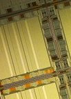
International SoC Conference In Pictures. . .
|
 |
|
If you
have any questions or need more information, please contact:
SoC@SavantCompany.com
or
949-851-1714 ― Thank
you!
a
|
|
* Program is subject to change.
SoC Conference Organizing Committee, Technical Advisory Board (TAB), and Savant Company Inc. reserves the rights to revise or modify the
SoC Conference program at
its sole discretion.
|
Click Here To
Download The UCI Campus Map
Directions &
Parking for Calit2 Building at the University of California, Irvine (UCI)
|
|
|
|
|
|
|
|
Day
One Wednesday October 23, 2013
SoC Conference Program Agenda* |
|
|
|
Savant
Company Inc.
 |
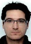
 Farhad
Mafie, SoC Conference Chairman,
IEEE OC SSCS & OCEN Chairs. Farhad
Mafie, SoC Conference Chairman,
IEEE OC SSCS & OCEN Chairs.
Welcome and Opening Remarks, Technology/Market Trends.
Farhad Mafie is SoC Conference
Chairman. He has over
20 years of experience in semiconductor and computer businesses and more
than 10 years of university-level teaching experience. He is the former Vice
President of Marketing and Engineering at Toshiba Semiconductor. He has also
worked in strategic marketing, project and design engineering at Lucent
Technologies, Unisys, and MSI Data. Farhad has a Master of Science and a
Bachelor of Science degree in Electronic Engineering from California State
University, Fullerton. He is an author and a translator, and his articles
have been published in a variety of journals and Web-based magazines on
technology and political affairs. In 2003, he published the biography of
Iranian poet and Nobel nominee who lived in exile, Nader Naderpour
(1929-2000), Iranian Poet, Thinker, Patriot. Farhad is also Editor-in-Chief
for the CRC Press SoC Design and Technologies Book Series, which includes
(1) Low-Power NoC for High-Performance SoC Design and (2) Design of
Cost-Efficient Interconnect Processing Units. Farhad is an active member of
IEEE, and he is the chair of IEEE Orange County Solid-State Circuits Society
(SSCS), as well as IEEE Orange County Entrepreneurs' Network (OCEN). He is
also a member of two UCI Advisory Committees: Communication System
Engineering and Embedded System Engineering Certificate Programs.
|
|
|
|
|
Analog and Mixed-Signal, SOI, and
FinFET Technologies, Trends
and Challenges for Complex SoC Designs.
Track
Chairman: Farhad Mafie, SoC Conference Chairman.
|
|
|
|
Sierra Nevada Corporation
|
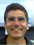
 Dr. Vladimir
Litvinov, Principal Scientist. Dr. Vladimir
Litvinov, Principal Scientist.
GaN Spintronics.
Abstract: We discuss
gate-controlled spintronic applications of wide bandgap GaN-based
semiconductors and compare them to their GaAs-based counterparts. Magnitude
of Rashba interaction and its role in electrically driven magnetic
properties of cubic and wirtzite III-V quantum wells are addressed in this
presentation in relation to spin injection efficiency. High spin injection
efficiency is the prerequisite of any voltage-controlled spin device. New
materials as topological insulators are discussed with respect to their
spintronic applications.
Bio: Dr. V.I. Litvinov.
Graduated from Lvov University (Radiophysics Department, Lvov, Ukraine),
hold PhD degree in Solid State Theory (Chernovtsy University, Ukraine) and
Habilitation Doctor degree in Physics and Mathematics (Institute of Physics,
Estonian Academy of Science, Tartu, Estonia). Since 1978 he was a head of
theoretical lab at the Institute of Material Science Problems, Academy of
Science of Ukraine. In 1996-1999 he worked as a Senior Research Associate at
the Department of Electrical & Computer Engineering, Northwestern
University, Evanston, IL (USA). He joined Sierra Nevada Corporation in 1999.
His areas of expertise include theory and modeling in semiconductor physics,
III-V and IV-VI semiconductor optoelectronic devices, superlattices,
metallic magnetic multilayers, and millimeter wave devices and antennas. Dr.
Litvinov has served as a principal investigator on projects supported by the
U.S. Air Force, SOCOM, U.S. Army, U.S. Navy, NASA, and MDA. He is a member
of IEEE, American Physical Society, and Material Research Society. He has
authored or coauthored more than 150 publications in peer-reviewed journals
and conference papers.
|
|
|
|
SOITEC
 |
 Bich-Yen NGUYEN,
SOITEC Bich-Yen NGUYEN,
SOITEC
“Fully Depleted SOI devices for SoC."
Abstract: Fully Depleted SOI (FDSOI)
devices have been developed in the last 20 years by academia and industry.
Their benefits have been demonstrated including better immunity to short
channel effects, lowest thresthold voltage variation due to minimizing the
random doping fluctuation. More important, FDSOI devices on ultra-thin BOX (UTBOX)
address a major challenge of the undoped channel devices, i.e. fabricate
multiple threshold voltage, VT, requirement for SoC application. The
ultra-thin-body and thin BOX (UTBB) devices feature the multi Vt-option with
simpler integration by using the combination of top gate work function and
ground plane doping type (N+ or P+ dopant). Additional special feature of
the UTBB device is the back gate bias which can be utilized for further
reducing the leakage or enhancing performance with dynamic VT modulation.
FD-SOI is an evolutionary innovation because it has the advantage of being a
planar fully depleted transistor which offers a minimum disruption design
change and simpler integration for cost effective mobile SoC application.
Bio: Bich-Yen Nguyen recently
joined Soitec as a Senior Fellow supporting the technology development of
new microelectronic devices and applications. Bich-Yen is also responsible
for the Strategic Microelectronic Technology and Marking. Prior to joining
Soitec, Bich-Yen was a senior manager at Freescale Semiconductor and a
Freescale/Motorola Dan Noble Fellow. Bich-Yen has been recognized for her
leadership and research in developing Freescale/Motorola's CMOS technology
for advanced integrated circuit products. She also was instrumental in
transferring process technology to production since 1980. Her honors and
awards include recipient of Dan Noble Fellow in 2001, the highest technical
award in Motorola, Master of Innovation Award in 2003. In 2004, she received
the 1st National Award “Women in Technology Lifetime Achievement Award”. She
holds over 130 worldwide patents and has authored more than 150 technical
papers on IC process, integration and device technologies. |
|
|
|
X-FAB
Semiconductor Foundries AG
 |
 Charles
Hage, Vice President of Business Development at X-FAB Semiconductor
Foundries AG. Charles
Hage, Vice President of Business Development at X-FAB Semiconductor
Foundries AG.
Complex Analog/Mixed-Signal SoCs - Why do more than 50% of the designs fail
in the first iteration? Foundry Perspective on first-time-right performance
for complex A/MS SoCs.
Abstract: Achieving first-time
right functional silicon in the first design iteration has become almost
commonplace in the realm of digital IC design. The same does not hold true
for analog/mixed-signal SoC designs. Although is it well understood what the
challenges as well the solutions are to achieve first-time-right – only
about 50% of all designs actually reach this important goal. This talk will
cover the challenges involved in achieving first-time-right for
analog/mixed-signal SoC designs, report on implementation issues and will
discuss current performance metrics. It will highlight the ecosystem with
all relevant market participants that are involved in the IC design process
and their contribution required in achieving first-time-right. X-FAB as
pure-play foundry is in the unique position to gauge and help
first-time-right performance and therefore has a good insight into how many
design iterations are typical for what type of designs. Differences in
first-time-right performance with respect to applications, markets and
regions will be discussed as well as the most common reasons for design
failure.
Bio: Charles Hage, Vice
President of Business Development at X FAB. In his early days, Charles
worked as a mixed signal design engineer for AMS and was later responsible
for the design center south Germany from 1995 till 1999 when working for
Thesys Mikroelektronik in Munich. Charles holds a Masters degree in
electrical engineering with specialization in electronics and wave
propagation from the University of Technology in Graz, Austria. |
|
|
|
Morning Break |
Morning Break |
|
|
|
STMicroelectronics
 |
 Dr. Fred
Gianesello. Dr. Fred
Gianesello.
Low Cost Front End Module
Integration on CMOS: the Era of SOI Technology.
Abstract: During past
years, RF ICs have achieved a very high level of integration in CMOS
technology integrating highly dense digital function as well as high
performances RF and analog ones (modern WiFi combo chip is a good example).
The next challenge concerns now the development of low cost Front End Module
(Power Amplifiers, switches, filters …) in CMOS technology. In this trend,
SOI technology has emerged as a promising one enabling the introduction of
high performances and low cost antenna switches on the market. This talk
will propose an overview concerning the challenges posed by 3G/4G FEM and
discuss how CMOS SOI technology enables to address those challenges.
Bio: Dr. Fred Gianesello received the B.S. and M.S. degree in Electronics
Engineering from Institut national polytechnique de Grenoble (Grenoble,
France) in 2003 and the Ph.D. degrees in electrical engineering from the
Joseph Fourier University (Grenoble, France) in 2006. Dr Gianesello has
authored and coauthored more than 100 refereed journal and conference
technical articles. He is currently working for STMicroelecetronics in
Crolles (France) where he leads the team responsible for the development of
electromagnetic devices (inductor, balun, transmission line, antenna, ...)
integrated on advanced RF CMOS/BiMOS (down to 14 nm), Silicon Photonics and
advanced packaging technologies (3D Integration, FOWLP, ...).
|
|
|
|
Microsemi
 |
 Dr.
Richard Newell, Senior Principal Product Architect, SoC Products Group,
Microsemi Corporation. Dr.
Richard Newell, Senior Principal Product Architect, SoC Products Group,
Microsemi Corporation.
Recent Advances in FPGA Design Security Reduce Insider Threats.
Abstract: Recent
advances in FPGA security architectures show the promise of reducing insider
threats at several stages of the supply chain. These include threats from
insiders at the device manufacturer, overbuilding devices or selling "floor
sweepings" (failed parts); through distribution, where parts may be
re-marked with more expensive model numbers and sold to unsuspecting systems
houses; to the end-user's manufacturing plant where there may be insiders
over-building at the system-level or installing malicious code in place of
the user's own design. From random bit generators to PUFs and elliptic
curve cryptography, this talk will show how all the pieces fit together in a
modern FPGA designed with enhanced security features to thwart the insider
threat.
Bio: Richard Newell is
Senior Principal Product Architect at Microsemi Corporation, SoC Products
Group where he has been active in planning the security features for the
next generation of Flash-based FPGAs and customizable System-on-Chips (cSoCs)
as well as expanding the available solutions for Microsemi’s current device
families. Richard has an electrical engineering background, with experience
in analog and digital signal processing, cryptography, control systems,
inertial sensors and systems, and FPGAs. He is an alumni of the University
of Iowa. He is the recipient of approximately one dozen U.S. patents and is
a member of the Tau Beta Pi and Eta Kappa Nu honorary engineering societies.
|
|
|
|
IBM
 |
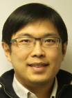 Dr.
Chung-Hsun Lin, Manager, Exploratory Device Research. IBM T.J. Watson
Research Center. Dr.
Chung-Hsun Lin, Manager, Exploratory Device Research. IBM T.J. Watson
Research Center.
FinFET Technology for SoC
Application.
Abstract: FinFET has been
adopted to extend CMOS scaling beyond the sub-22nm node because of superior
electrostatic control and lower sensitivity to random dopant fluctuations (RDF).
This enables a very robust low-Vdd design spectrum. However, practical
challenges and process complexity issues exist in the integration of FinFET
structures at relevant technology dimensions. In this
talk, we will address the device design consideration for SoC application,
including, variability mitigation, multiple Vt tuning, and passive elements
design, in FinFET technology for 14nm node and beyond.
Bio: Dr. Chung-Hsun Lin received the B.S. and M.S. degrees in Electrical
Engineering from National Taiwan University in 1999 and 2001, and the Ph.D.
degree in Electrical Engineering from the University of California,
Berkeley, in 2007. His Ph.D. work on FinFET compact modeling along with
colleagues at UC Berkeley lead to the world first industrial standard FinFET
SPICE model – BSIM-CMG. He joined IBM T.J. Watson Research Center in 2008 as
a Research Staff Member in the area of CMOS technology and device modeling.
He was involved in early FinFET device design study, TCAD/compact modeling
and technology target definition, 22nm PDSOI technology bring up and
power-performance optimization with colleagues at IBM. He is currently
managing the exploratory device research group. Dr. Lin is a
recipient/co-recipient of 2011 SRC Outstanding Industry Liaison Award. He
was elected as IBM Master Inventor in 2012 for outstanding contribution to
corporate's IP portfolio. He has authored or coauthored more than 70
technical papers and holds more than 25 US patents.
|
|
|
|
Microsemi
Keynote
|
 Jim
Aralis, Chief Technology Officer (CTO), and Vice President of R&D. Jim
Aralis, Chief Technology Officer (CTO), and Vice President of R&D.
Keynote:
"Living on the Edge (of the SoC)"
Abstract: This
presentation will outline the new process, processor, and packaging
technologies that are enabling the expansion of mixed-signal SoC product
development efforts. Subjects that will be covered include the optimization
of design methodologies, mode partitioning, and process selection to
maximize cost-savings, performance, and time-to-market. The presenter will
also discuss how expertise in analog processing, signal conditioning,
precision timing, and high speed wired and wireless communications design
remain critical for designing differentiated products in an expanding and
evolving digital environment.
Bio: Jim Aralis has served as
chief technology officer and vice president of R&D for Microsemi since
January 2007. He has more than 30 years experience in developing custom
analog device and process technologies, analog and mixed-signal ICs and
systems, and CAD systems.
Jim played a key role in transitioning Microsemi to a virtually fabless
model, supporting multiple process technologies including, high voltage and
high power BCD/CMOS, high power high integration CMOS, GaAs, SiGe, IPD, RF
CMOS SoI, GaN, SiC, and several high-density packaging technologies.
From 2000 to 2007, Jim established and served as senior design director of
Maxim Integrated Product’s engineering center in Irvine, Calif. Before that,
he spent 7 years with Texas Instruments/ Silicon Systems as mixed-signal
design head and senior principal engineer. Additional experience includes 11
years with Hughes Aircraft Company in positions of increasing responsibility
including senior scientist. Jim earned a bachelor of science degree in
Math Applied Science and Physics and a master of science in electrical
engineering from UCLA. He holds 9 patents for circuit and system design.
|
|
|
|
Lunch |
Lunch |
|
|
|
Nokia
Keynote
 |
 Dr.
John Paul Shen, Nokia Fellow, Founding Head of Nokia Research North America
Lab. Dr.
John Paul Shen, Nokia Fellow, Founding Head of Nokia Research North America
Lab.
Mobile Computing Mega Trends and Major Challenges.
Abstract: This talk highlights
four mega trends for mobile computing and the associated challenges. (1)
Mobility Dominates: mobile devices will be the technology and innovation
driver; (2) Wireless Clouds: the dominant edge of the cloud will become
wireless; (3) Big Data Curating: inundation of massive amounts of real-time
mobile data; (4) Energy Efficiency: improving the ratio of {UserExperience/(EnergyxCost)}
becomes the new scaling law of 2X every 2 years.
Bio: John P. Shen is a Nokia
Fellow (7th in the company) and was the founding director of Nokia Research
Center - North America Lab (formerly NRC Palo Alto) with research teams
pursuing a very wide range of research projects in mobility and mobile
computing. Prior to joining Nokia in 2006, John was the Director of the
Microarchitecture Research Lab at Intel. Prior to joining Intel in 2000,
John was a tenured Full Professor in the Electrical and Computer Engineering
Department at Carnegie Mellon University, where he supervised a total of 17
PhD students and dozens of MS students, received multiple teaching awards,
and published two books and more than 100 research papers. One of his books,
“Modern Processor Design: Fundamentals of Superscalar Processors”
(McGraw-Hill 2005) is still being used in the EE382 Advanced Processor
Architecture course at Stanford University. He is currently an adjunct
professor at the CMU Silicon Valley campus.
|
|
|
|
Intel
 |
 Dr.
Jeff Parkhurst, Program Director, Intel Science and Technology Centers. Dr.
Jeff Parkhurst, Program Director, Intel Science and Technology Centers.
SoC Platform Opportunities and Challenges in the Big Data Economy.”
Abstract: Processing Big Data has been traditionally done at the Cloud
Level. However, the paradigm is shifting as the need to both mine and
process Big Data at the edge becomes paramount. This talk will explore a new
Big Data ecosystem and discuss how it intersects with current SoC platforms
including exploring future opportunities and challenges.
Bio: Dr. Jeff Parkhurst is the Program Director for three Intel Science and
Technology Centers focusing on Embedded Computing, Cloud Computing and Big
Data. He is responsible for managing the operational details in each center
as well as aiding in direction setting of the research. The Program Director
is the primary liaison between Intel and the universities on all operational
matters including contracts, IP, space, logistics, funding, and
technology/knowledge transfer. Prior to this assignment, Jeff was an
Academic Research Programs Manager working with senior technologists
internal and external to Intel setting research directions for the design
science areas of the Semiconductor Research Corporation (SRC). Jeff received
his BS from University of Nevada at Reno in 1983 and his MS from the
University of California at Davis in 1988 and his PhD at Purdue University
in 1994. Dr. Parkhurst is the author of numerous papers and one patent.
|
|
| |
University of Pennsylvania
Keynote
 |
Dr. Nader Engheta, H. Nedwill Ramsey Professor of
Electrical and Systems Engineering, and Professor of Bioengineering.
University of Pennsylvania
"Seeing the Unseen: From
polarization-sensitive eyes in nature to system-on-chip sensing and imaging
devices."
Abstract:
Certain animal species in nature have visual systems that are sensitive to
light’s polarization – a capability that is lacking in the human eyes. The
species with polarization vision can detect this characteristic of
image-forming light and can extract its information. Polarization is
obviously an important feature of optical signals, and can be affected by
surface shapes, materials, local curvature, and relative location of sources
and objects, and thus it can provide useful information about the observed
scene and objects. What can one learn from this interesting ability of
polarization sensing and detection in nature that has been evolved in
certain biological visual systems? Understanding the biophysical mechanism
behind the polarization vision and reverse engineering its functionality
leads to exciting novel methods and techniques in sensing and imaging with
various applications. Inspired by the features of polarization-sensitive
visual systems in nature, we have been developing various man-made,
non-invasive imaging methodologies, sensing schemes and visualization and
display schemes that have shown exciting and promising outcomes with useful
applications in system design in the optical and microwave domains. These
techniques provide better target detection, enhanced visibility in otherwise
low-contrast conditions, longer detection range in scattering media,
polarization-sensitive adaptation based on changing environments, surface
deformation-variation detection, “seeing” objects in shadows, and other
novel outcomes and applications. In this talk, I will discuss several
optical aspects of the biophysical mechanisms of polarization vision, and
present sample results of our bio-inspired imaging methodologies. (In
collaboration with Professor Jan Van der Spiegel’s group at UPenn.)
Bio: Recipient of 2013 SINA Award in Engineering and 2012 IEEE
Electromagnetics Award, Nader Engheta is the H. Nedwill Ramsey Professor at
the University of Pennsylvania with affiliations in the Departments of
Electrical and Systems Engineering, Bioengineering, Physics and Astronomy,
and Materials Science and Engineering. He received his B.S. degree from the
University of Tehran, and his M.S and Ph.D. degrees from Caltech. Selected
as one of the Scientific American Magazine 50 Leaders in Science and
Technology in 2006 for developing the concept of optical lumped nanocircuits,
he is a Guggenheim Fellow, an IEEE Third Millennium Medalist, a Fellow of
IEEE, American Physical Society (APS), Optical Society of America (OSA),
American Association for the Advancement of Science (AAAS), and SPIE-The
International Society for Optical Engineering, and the recipient of 2013
Benjamin Franklin Key Award, 2008 George H. Heilmeier Award for Excellence
in Research, the Fulbright Naples Chair Award, NSF Presidential Young
Investigator award, the UPS Foundation Distinguished Educator term Chair,
and several teaching awards including the Christian F. and Mary R. Lindback
Foundation Award, S. Reid Warren, Jr. Award and W. M. Keck Foundation Award.
His current research activities span a broad range of areas including
metamaterials, nanophotonics, graphene optics, imaging and sensing inspired
by eyes of animal species, optical nanoengineering, microwave and optical
antennas, fractional operators in physics, and engineering and physics of
fields and waves. He has co-edited the book entitled “Metamaterials: Physics
and Engineering Explorations” by Wiley-IEEE Press, 2006. He was the Chair of
the Gordon Research Conference on Plasmonics in June 2012. |
|
|
|
Morning Break |
Afternoon Break |
|
|
|
|
Emerging & Leading-Edge
Communication ICs, High-Speed I/Os & NoC Optical Communications.
Track
Chairman: Dr. Yasuo Hidaka is a senior researcher in Platform
Technology Innovation Group at Fujitsu Laboratories of America.
|
|
|
|
Pohang University
of Science and Technology
(Korea)
 |

Professor Byungsub Kim.
Revisiting High-Speed Interconnect Channel Modeling.
Abstract: In this talk,
modeling and analysis of RC-dominant wires for high-speed wireline
transceiver design will be explained. A closed form formula derived from
telegrapher’s equation accurately describes a frequency response of an
RC-dominant wire, yet it is simple and intuitive for designers to easily
understand design trade-offs without a complex numerical equation solver.
This talk will also give explanation on how the model is derived and how it
can help designers in example transceiver designs,
Bio: TBD.
|
|
|
|
Fujitsu Laboratories of America, Inc.
 |
 Dr. Yasuo Hidaka. Dr. Yasuo Hidaka.
Low-Frequency Equalizer for High-Speed I/O.
Abstract: Equalizers are
commonly used for multi-Gbps high-speed I/O in SoC in order to cancel ISI
(inter-symbol interference) caused by frequency-dependent channel loss.
Conventional equalizers such as FFE, CTLE, and DFE are quite effective for
large high-frequency loss which often exceeds 30-40dB at Nyquist frequency
for 10+Gbps. However, we also need to compensate for a small amount of loss
at low frequency (e.g. 100 to 500MHz), because the skin effect in PCB starts
at very low frequency (e.g. < 10MHz). Conventional equalizers cannot
compensate for the low-frequency loss, because the slope of the
low-frequency loss is too gentle (<3dB/dec) for FFE and CTLE which do not
have a pole in low frequency and hence have only a steep (20dB/dec) slope
above zero, and DFE cancels only short-term ISI. The low-frequency loss has
often been overlooked or neglected, because 1) the loss is small (2 to 3dB),
2) the low-frequency loss is degenerated at DC and hardly recognized with a
linear frequency axis which is the best to observe frequency dependence of
skin effect and dielectric loss, 3) the long ISI tail in time-domain pulse
response seems well cancelled at first glance by conventional equalizers
only. However, the best link performance achieved by conventional equalizers
has been significantly limited by lack of compensation for the small
low-frequency loss. This presentation will demonstrate the performance
advantage of the low-frequency equalizer which we have implemented together
with CTLE and 2-tap DFE for high-frequency loss in our 32Gbps receiver using
28nm CMOS technology.
Bio: Dr. Yasuo Hidaka is a
senior researcher in Platform Technology Innovation Group at Fujitsu
Laboratories of America, Sunnyvale, California. At FLA, he is working on
research and development of high-speed interconnect technologies for Fujitsu
Servers, primarily focusing on signal integrity problems of electrical
interconnect from both sides of transmission channel and I/O circuit. He has
acquired a broad range of in-depth experience and knowledge in his career in
computer science, electrical engineering, and mechanical engineering,
including but not limited to mixed-signal analog circuit, digital/analog
signal processing, logic design and verification, high-speed analog circuit,
adaptive control theory, IC layout design, wireless circuit, microwave
engineering, ESD design, system bring up, chip characterization,
manufacturing test, high-speed PCB design, processor architecture, parallel
computer architecture, compilers, programming languages, operating systems,
solid modeling, computer graphics, internet protocol, queuing theory,
classical control theory, modern control theory, optimal control theory,
statistical analysis, reliability analysis, device physics. He received his
Ph.D. in Information Engineering from University of Tokyo in 1995 where his
research focused on parallel computer architecture. He received M. Eng. in
Information Engineering and B. Eng. in Precision Machinery both from
University of Tokyo in 1991 and 1989, respectively. He co-authored 2 books,
authored or co-authored 13 journal papers, and 14 peer-reviewed conference
papers including 5 papers in ISSCC and 1 paper in ISCA which are top
international conferences in the areas of circuit design and computer
architecture, respectively. He holds 30 granted U.S. patents.
|
|
|
|
UCLA
 |
 Dr. Brandon
Buckley. Dr. Brandon
Buckley.
Coherent Dispersive Fourier Transform for Real-time Digitization
Abstract: Photonic
time-stretch boosts the performance of analog-to-digital converters and
digital signal processors by slowing down wideband analog signals before
digitization. Real-time burst sampling rates exceeding 1 TSps have been
demonstrated, along with similarly high-throughput digital processing.
Additionally, by reducing effective aperture jitter, time-stretch
transformation offers superior amplitude and temporal resolution across
ultra-wide analog bandwidths. These capabilities are critical for
high-performance applications such as signal integrity monitoring in optical
networks, radar and electronic intelligence, and high-throughput screening
in medicine and bio-defense. Recently, we have developed the coherent
dispersive Fourier transformation, which enables real-time recovery of phase
and amplitude information encoded on broadband optical pulses. By adapting
this technology as a coherent receiver in photonic time-stretch, we are able
to digitally compensate for non-linear distortions and dispersion induced
fading. Here I will present our most recent results and discuss the impact
on high-performance analog-to-digital conversion and signal processing.
Bio: Dr. Brandon W. Buckley
received his B.A. degree from Cornell University in 2007 and his M.S. and
Ph.D. degrees from University of California, Los Angeles in 2009 and 2013,
all in physics. In 2011, he spent a year at Intel Labs in Santa Clara, CA as
a member of their Silicon Photonics Group. Brandon is currently a postdoc in
Dr. Bahram Jalali’s Photonics Laboratory at UCLA developing ultra-fast
optical instruments. His research interests include photonic enhanced
analog-to-digital conversion and signal processing, integrated optics, and
high-speed biomedical imaging.
|
|
|
|
Purdue
University
 |
 Dr. Byunghoo
Jung, Associate Professor, School of Electrical and Computer Engineering,
Purdue University. Dr. Byunghoo
Jung, Associate Professor, School of Electrical and Computer Engineering,
Purdue University.
Wireless Links in 3-D ICs – The On-Chip Wide-Band Microbump Antenna Way
Abstract: Three-dimensional
integrated circuit (3-D IC) technology for improving integration density has
made great progress, and its wide deployment in high performance computing
systems has been envisaged during the recent years. For successful
deployment, chip-scale network configuration and I/O connectivity are
particularly important because of its strong correlation with architectural
flexibility and expandability. Despite the high integration density in 3-D
IC, there is a stringent constraint in its both internal and external
connectivity. Wireless communication links between 3-D ICs provides a
promising perspective for reducing latency and overall pin count. One of the
biggest challenges in wireless links is a Si-compatible on-chip antenna with
low cost and area overheads and high efficiency. Recently, an idea of using
fully Si-compatible microbumps placed between the layers of 3-D IC as a
high-efficiency, compact, and wide-bandwidth antenna was demonstrated. The
wide-bandwidth microbump antenna allows a highly flexible wireless link with
a data capacity comparable to that of a wireline link and shows high
invariability over process variation. This opens an interesting paradigm of
utilizing the wireless I/Os in future high-performance 3-D IC systems to
improve the expandability and connectivity, while minimizing I/O pin counts
and latency. This also offers a possibility of providing non-invasive
wireless testing for 3-D ICs.
Bio: Byunghoo Jung received the B.S. degree from Yonsei University, Korea,
in 1990, the M.S. degree from KAIST, Korea, in 1992, and the Ph.D. degree
from the University of Minnesota, Twin Cities, in 2005. From 1992 to 1999,
he was with Samsung Electronics, Korea, where he was involved in the design
of video signal driver circuits for flat panel display. Following receipt of
his PhD in January 2005, he was with Qualcomm in San Diego as a Senior RF
Design Engineer until he joined the School of Electrical and Computer
Engineering at Purdue University in August 2005. His research interests
include analog, mixed signal, and RF circuit design for wireless and wired
communications and biomedical applications. He is the first place winner of
the 2002-2003 SRC SiGe BiCMOS Design Challenge (as a lead designer) and the
2007-2008 SRC/SIA IC Design Challenge (as a lead faculty). He has served as
a Co-Chair of the DAC/ISSCC Student Design Challenge, and as an Associate
Editor of the IEEE Transactions on VLSI Systems. He is a member of the
Analog Signal Processing Technical Program Committee in the IEEE Circuits
and System Society.
|
|
|
|
OPEN Alliance

Broadcom
 |
Dr. Ali Abaye, Senior Director of Product Marketing for the Infrastructure &
Networking Group.
OPEN Alliance: Supporting the Standardization of Automotive Ethernet.
Abstract: In-vehicle
electronics are growing in number and complexity, keeping step with
technology advancements and capitalizing on consumer expectations for a
connected driving experience. As a result of the significant increase in
volume and complexity of in-car electronics, demand for networking solutions
that offer low-cost, high speed transmission and bandwidth is on the rise.
Standardization is essential as a major enabler for new and innovative
in-vehicle applications, allowing automotive manufacturers to meet customer
expectations and keep the bottom line in check. This presentation, delivered
by Dr. Ali Abaye, Senior Director of Automotive and PHY Products at Broadcom
and founding member of the OPEN Alliance SIG, explores the role of Ethernet
in enabling advanced driver assistance, safety and infotainment features in
next generation automotive networks and the role of the OPEN Alliance SIG.
Bio: Dr. Ali Abaye serves as
Senior Director of Product Marketing for the Infrastructure & Networking
Group at Broadcom Corporation, responsible for the company’s networking
portfolio of automotive devices and 1G and 10G copper physical layer
transceivers (PHYs). Prior to Broadcom, Dr. Abaye served as System Architect
for the Broadband and Wireless System Engineering division at Nortel. Prior
to Nortel, he held various technical and strategic marketing positions at
Centillium Communications. Dr. Abaye holds a Ph.D. in Electrical Engineering
from Southern Methodist University in Dallas, Texas.
|
|
|
|
Università
di Ferrara
 |
 Professor
Luca Ramini, Università di Ferrara. Professor
Luca Ramini, Università di Ferrara.
Optical Interconnect Technology for 3D Stacked Multi- and Many-Core Systems:
When, Where and How.
Abstract: Optical
Networks-on-Chip (ONoCs) are considered a promising way of improving power
and bandwidth limitations in next generation multi- and many-core integrated
systems. Today, many research works on optical on-chip networks have been
proposed in the recent literature, however, they are fundamentally still at
the stage of a promising research concept, thus neglecting cross-layer
design issues. This presented talk focuses on Optical NoC topologies,
especially wavelength-routed ones (WRONoCs), for 3D stacked systems, and
addresses the design predictability gap when moving from abstract logic
schemes of interconnect topologies to their physical implementation. In
light of this, the work discloses the key role of placement and routing
constraints for optical on-chip networks as a way of emphasizing the gap
between the Optical Network-on-Chip (ONoC) concept and a viable interconnect
technology with practical relevance. In addition, the robustness of
ONoC topologies to such constraints, and different implementation
workarounds such as global connectivity and network partitioning will be
discussed. Finally, the presented work makes interesting insights into the
comparison between optical filter-based topologies vs.
spatial-division-multiplexing ring topologies, by assessing physical design
trade-offs of an engineered optical layer for a 3D-stacked multi-core
processor.
Bio: Luca received the M.S.
degree in engineering and technologies for Telecommunications and
Electronics in the 2010. His first studies on Silicon Photonics Technology
have been started during his master thesis entitled “ Modeling of
microcavities based on photonic crystal technology”. Since June 2010 Luca is
working in the MPSoC Research Group under the supervision of the professor
Davide Bertozzi at the Engineering Department of the University of Ferrara,
in Italy. Luca has started his PhD degree on January first 2011 which is
completely funded by the Photonica Project. His current research interests
include design of photonics interconnect networks and modeling and
simulation of photonics devices for multi-processor system on chip. Luca has
expertise on the FDTD Method, which is mainly utilized for the modeling at
physical level of photonic switching elements, and on the SystemC simulation
framework for the characterization at system level of Optical
Networks-on-Chip. Luca’s current research is focused on a design space
exploration of Wavelength-Routed optical NoC topologies for a 3D-Stacked
Multi-Core processor of practical relevance, leveraging on Place and Route
Constraints to quantify the deviation between logic topologies and
corresponding physical ones in terms of insertion loss, delays and power.
Since June to December 2011, Luca visited the research group of Professor
Luca Carloni at Columbia University in the city of New-York. Luca has also
presented and shared his research interests at several international
conferences and workshops, among the most recent we remember: Asia
Communication and Photonics Conference’12 in Guangzhou (China), DATE’13
conference in Grenoble (France) as well as the latest CMOS’13 Emerging
Technologies Research symposium in Whistler (Canada). Luca is finally
co-author of seven publications focused on optical Networks-on-Chip and he
is currently writing his first book chapter on this emerging technology as
well. |
|
|
|
|
|
|
|
|
|
Day TWO Thursday, October 24, 2013
SoC Conference Program Agenda* |
|
|
|
Savant
Company Inc.
|
Farhad
Mafie, SoC Conference Chairman,
IEEE OC SSCS & OCEN Chairs.
Bio: Farhad Mafie is SoC Conference
Chairman. He has over
20 years of experience in semiconductor and computer businesses and more
than 10 years of university-level teaching experience. He is the former Vice
President of Marketing and Engineering at Toshiba Semiconductor. He has also
worked in strategic marketing, project and design engineering at Lucent
Technologies, Unisys, and MSI Data. Farhad has a Master of Science and a
Bachelor of Science degree in Electronic Engineering from California State
University, Fullerton. He is an author and a translator, and his articles
have been published in a variety of journals and Web-based magazines on
technology and political affairs. In 2003, he published the biography of
Iranian poet and Nobel nominee who lived in exile, Nader Naderpour
(1929-2000), Iranian Poet, Thinker, Patriot. Farhad is also Editor-in-Chief
for the CRC Press SoC Design and Technologies Book Series, which includes
(1) Low-Power NoC for High-Performance SoC Design and (2) Design of
Cost-Efficient Interconnect Processing Units. Farhad is an active member of
IEEE, and he is the chair of IEEE Orange County Solid-State Circuits Society
(SSCS), as well as IEEE Orange County Entrepreneurs' Network (OCEN). He is
also a member of two UCI Advisory Committees: Communication System
Engineering and Embedded System Engineering Certificate Programs.
|
|
|
|
|
Leading-Edge Technologies and Design Methodologies & Approaches for Emerging Complex SoCs.
Track
Chairman: Dr. Wakaba K. Wakabayashi. NEC.
|
|
|
|
Semtech
Corporation
 |

Dr. Amr Fahim, Principal Design Engineer.
Efficient and Accurate Frequency Synthesizer Model for SoC Processors.
Abstract: Transient domain
simulation is a critical step in the verification flow of system-on-a-chip
(SoC) processors. This is often complicated by the presence of custom analog
circuitry on the chip that must be taken into account. One such block that
is needed in virtually all SoC processors is the phase-locked loop (PLL). In
conventional Verilog-based methodologies, the PLL functionality is bypassed
and replaced with a very crude functional model. Although, this may be
sufficient for basic static functionality, it completely ignores the loop
dynamics, which may be critical to model. There have been recent attempts in
providing some PLL functionality, but on the expense of a much longer
simulation time. In this paper, a novel method of modeling a phase-locked
loop that is suitable for system-on-a-chip (SoC) processors is described. A
computationally efficient and accurate model of a PLL is described.
Simulations show that transistor level accuracy is achieved with orders of
magnitude is speed-up. In addition to functionality, jitter is also
accurately predicted as compared to measured results.
Bio: Dr. Amr Fahim received his B.A.Sc. degree in computer engineering and
M.A.Sc. and Ph.D. degrees in electrical engineering from the University of
Waterloo, Ontario, Canada in 1996, 1997 and 2000 respectively. He has over
17 years of experience in design of RF/mixed-signal IC design for
system-on-a-chip (SoC) processors for both wireless and wireline products,
developing innovative solutions to meet the demands of these markets. He is
the author of over 25 papers and 15 patents. He is also the author of the
text book entitled "Clock Generators for SoC Processors" and has been a
reviewer and Associate Editor for several IEEE journals including the
Journal of Solid-State Circuits, IEEE Transactions on Circuits and Systems
II, and the IEEE Transactions on VLSI. He is currently with Semtech
Corporation, Irvine, CA. His research interests include frequency
synthesizers and RF/mixed-signal SoC integration.
|
|
|
|
Spansion Inc.
 |
 Shiva
Shetty, Director of R&D Product Engineering Group at Spansion. Shiva
Shetty, Director of R&D Product Engineering Group at Spansion.
Advancement in Charge-Trap Flash Memory Technology.
Abstract: Charge-trap Flash
has been scaling effectively and successfully productized in high volume for
several technology generations. As a result of its high intrinsic
reliability, small cell size, and good performance at elevated temperatures,
charge-trap Flash has captured a significant portion of the market.
Two-bit-per-cell MirrorBit® charge-trap technology has been the industry
benchmark for NOR Flash for more than a decade, spanning six generations of
scaling, and is now ubiquitous in high-density parallel and serial NOR
applications. In fact, 45nm MirrorBit technology is in volume production
today with an 8Gb chip—the highest-density monolithic NOR flash in the
market. Meanwhile, 32nm MirrorBit cell has been demonstrated and will enable
even higher densities of monolithic NOR Flash. For NAND applications, the
industry’s first manufacturing-ready, charge-trap NAND technology called
Heterogeneous Charge Trap (HCT)TM NAND Flash has been recently developed.
For SoC products with ultra-fast read access time, embedded Charge Trap (eCT)TM
Flash is being developed and integrated with an advanced logic process. The
planar cell structures will enable continued scaling of these charge-trap
technologies, while new architectures such as 3D charge-trap Flash will
emerge and further extend the density-growth trend. This presentation will
cover technological advancements and key attributes of these charge-trap
technologies.
Bio: Shiva Shetty currently is director of R&D Product Engineering group at
Spansion, a leading provider of Flash memory based solutions. He leads a
team responsible for characterizing and qualifying test chips and products
on new technologies. He received his B.S degree from Indian Institute of
Technology, Bombay in 1996 and his M.S. in Electrical Engineering from
Rensselaer Polytechnic Institute, Troy, NY in 1998. Since then, he has
worked at AMD and Spansion and has been part the of various technology
development teams that developed and qualified several generations of logic
and flash memory technologies.
|
|
|
|
SP3 Diamond Technologies
 |
 Dr. Mario M.
Pelella. Dr. Mario M.
Pelella.
Ultimate Solution for 3D-IC Technologies.
Abstract: To continue the
insatiable performance and functionality gains of the last four decades,
while empowering future heterogeneous super systems on a package with
“More-than-Moore” integration, the development of a 3D-IC substrate platform
is essential and a key enabling technology that will fuel the growth of
Semiconductor industry over the next four decades. While the benefits are
clear (smaller footprint, reduced interconnect delays, lower power, and
higher bandwidth), the design complexities of 2D platforms are further
aggravated in a 3D environment due to yield, thermal management, TSV
integration, and design complexity concerns. Spatially elevated operating
temperatures within the 3D-IC stack, due to poor thermal conductivity of
conventional materials, aggravates the latency and timing between chips,
degrades reliability, and reduces the overall performance of the system.
Moreover, the most significant barrier to continued system performance
improvements today is power limitations. To circumvent these onerous thermal
management issues, a significantly higher thermal conductivity material
needs to be incorporated into the 3D-IC stack, which diamond films can
provide. The key attributes of diamond interposers include a CTE matched
stack, high Young’s modulus, high thermal conductivity, and compatibility
with existing copper damascene processing. Furthermore, to mitigate thermal
management issues and the integration costs of interposers, the utilization
of SOD (silicon-on-diamond) substrates within the 3D-IC stack would provide
the ultimate solution for 3D-IC technologies and can be available in wafer
sizes of 100 – 300mm to support the industry. The benefits and challenges of
incorporating diamond films into the 3D-IC stack will be analyzed and
discussed.
Bio: Dr. Mario Pelella, is the
company’s vice president of engineering. As the leader of Technology and
Process Solutions group, Mario is responsible for the development and
technical success of all sp3’s semiconductor and MEMS-related diamond
products. He previously served as director of technology solutions at SVTC
Technologies where he was responsible for developing SVTC’s technology
roadmap for the semiconductor, aerospace and defense, MEMS, life science,
photonic and energy industries. He has also held positions with tau-Metrix,
AMD and IBM. Mario earned his Ph.D. in Electrical Engineering from the
University of Florida and BSEE and MSEE degrees from Clarkson University. He
holds over 50 US patents and 15 worldwide patents and is the author of more
than 60 publications, including three that earned Best Paper awards.
|
|
|
|
Palmchip
 |
 Jauher
Zaidi, Chairman & CTO, Palmchip. Jauher
Zaidi, Chairman & CTO, Palmchip.
Securing the "Internet of Things”.
Abstract: The Internet of
Things (IOT) is the term for the phenomenon where people and things
(physical devices such vehicles, commercial and industrial equipment,
medical devices, remote sensors, etc.) are connected to networks that are
linked to the Internet and communicating vast amounts of valuable data.
While the idea is not new, the recent proliferation creates a sense of
urgency to better understand and develop edge devices which are secure.
Personal privacy and Security is huge concern. We must design IoT devices
with built in Security. IoT Security can not be a after thought. Cisco
reports over 50B devices will be connected to internet by 2020.
Bio:
Jauher Zaidi is Chairman & CTO of Palmchip Corporation. Jauher has over
twenty years of experience in system design and integration. Before founding
Palmchip in 1996, he was involved in system-on-chip (SoC) integration at
Quantum Corporation. Jauher received his BSEE and MSEE degrees from Pacific
States University in Los Angeles, California. He has also participated in
many SoC panels and is a recognized expert in the area of SoC development.
|
|
|
|
GLOBALFOUNDRIES
 |
 Dr. An Chen,
Senior member of Technical Staff. Dr. An Chen,
Senior member of Technical Staff.
Beyond-CMOS Devices for Low-Power System Design.
Abstract: Increasing power
density and heat dissipation with CMOS scaling have motivated the research
community to pursue low-power devices and designs. Although non-planar
structures and alternative channel materials improve electrostatics and help
to extend CMOS scaling, the fundamental switching energy limit in
conventional charge-based device models imposes ultimate energy constraints
in highly scaled CMOS devices. Switching devices based on unconventional
mechanisms or even alternative state variables have been explored to
circumvent this limit for low-power applications. Steep sub-threshold slope
(SS) devices either utilize internal gain or overcome thermal limit to
achieve <60mV/dec SS. Unconventional charge-based logic devices exploit
novel switching mechanisms different from conventional field-effects, e.g.,
tunneling transport, discrete quantum states, phase transition, Coulomb
coupling, etc. Non-charge state variables (e.g., spin) may also enable logic
operations that could potentially reach very lower power consumption.
Despite the promising low-power characteristics, these beyond-CMOS devices
also face different challenges, e.g., speed, material, scalability, etc.
Systematic benchmark of these beyond-CMOS devices has also revealed
performance-power tradeoffs. Interconnect solutions for beyond-CMOS devices
remain unproven. These challenges have to be addressed in circuit/system
designs that may utilize unique characteristics of these novel devices,
e.g., built-in nonvolatility in logic functions. Memory-logic integration
may enable more energy-efficient system designs. Emerging devices with
structures and materials compatible with CMOS have significant advantages.
Beyond-CMOS technologies may need to shift from device-centric toward
design-centric to overcome device-level limitations.
Bio: Dr. An Chen is a senior
member of technical staff at GLOBALFOUNDRIES, working on emerging logic and
memory technologies. He is the Technical Lead on emerging nonvolatile
memories in the Exploratory Research group. He received the Ph.D. degree in
Electrical Engineering from Yale University. He previously worked at
Spansion on emerging memories and at AMD as an assignee to the
Nanoelectronics Research Initiative. He is the chair of the Emerging
Research Device (ERD) chapter of the International Technology Roadmap of
Semiconductors (ITRS).
|
|
|
|
Morning Break
|
Morning Break |
|
|
|
NEC
ALDEC


|
 DR. Wakaba
K.Wakabayashi. DR. Wakaba
K.Wakabayashi.
FPGA+C-based HLS Can Outperform GPGPU (SIMD Processors) from the View Point
of Compiler and Architecture.
Abstract: TBD.
Bio: Dr. Kazutoshi Wakabayashi, received his B.E. and M.E. degrees and ph.D
from the University of Tokyo in 1984,1986 and 2006. He was a visiting
researcher at Stanford University during 1993 and 1994. He joined NEC
Corporation in Kawasaki Japan in 1986 and he is currently a Senior Principal
Researcher of Central Research Labs. NEC Corporation. Dr. Wakabayashi has
been engaged in the research and development of VLSI, CAD systems;
high-level and logic synthesis, formal and semi-formal verification,
system-level simulation, HDL, emulation, HLS and Floorplan links, and
reconfigurable computing. He served on executive committee or organizing
committee of some international conference including:
ASP-DAC'09 General Chair, CODES+ISSS'09 Co-Technical Program Chair. a
Secretary of Steering Committee of ASPDAC, and Executive Committee for ICCAD
and DAC, Tutorial Chair of ASPDAC2006, Steering Committee of ITC-CSCC (09-).
He has served on the program committees for several international
conferences including: DAC, ICCAD, DATE, ASP-DAC, ISSS, SASIMI, and ITC-CSCC,
ISCAS, VLSI-TSI, SBCCI, VLSI Design, ESS, ISLP and so on. Also, he has
served as a general chair, a secretary, and a Technical Program Committee
member for a number of Japanese conferences, including: Institute of
Electronics, Information and Communication Engineers of Japan (IEICE), the
Information Processing Society of Japan (IPSJ), System LSI WS, Karuizawa WS.
He is currently chair of SIG on VLSI design methodology of IEICE, and
elected member of IEICE. He was an associate editor of Transactions on IEICE
on VLSI CAD, DAEM. He is a rep. of CEDA (Council for EDA) of IEEE. He is
also a member of IEEE, IPSJ, and IEICE. He received the IPSJ Kiyasu
Special Industrial Achievement Award 2011, the Yamazaki-Teiichi Prize in
2004, and the IPSJ Convention Award in 1988, Sakai Kinen Special Award in
2001, and the NEC Distinguished Contribution Award in 1993 for his logic
synthesis system and in 1999 for his formal verification and in 2006 for his
High Level Synthesis. His C-based Synthesis and Verification tool suite
called "CybeWorkBench" received a Grand prize of "LSI of the Year 2003" and
"LSI of the Year 2007". |
|
|
|
UCI
 |
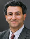
 Professor,
Nader Bagherzadeh, UCI, EECS. Professor,
Nader Bagherzadeh, UCI, EECS.
Exascale and Embedded Systems Have Common Goals?
Abstract: This talk will
address some of the challenges facing designers of embedded systems as well
as supercomputers. In particular the foci will be on power consumption and
performance issues that are considered as major hurdles in order to meet
design specification objectives.
Bio:
Dr. Nader Bagherzadeh has
been involved in research and development in the areas of computer
architecture, reconfigurable computing, VLSI chip design, and computer
graphics. For almost ten years ago, he was the first researcher working on
the VLSI design of a Very Long Instruction Word (VLIW) processor.
Since then, he has been working on multithreaded superscalars and their
application to signal processing and general purpose computing. His
current project at UC, Irvine is concerned with the design of coarse grain
reconfigurable pixel processors for video applications. The proposed
architecture, called MorphoSys, is versatile enough to be used for digital
signal processing tasks such as the ones encountered in wireless
communications and sonar processing. DARPA and NSF fund the MorphoSys
project (total support $1.5 million). Dr. Bagherzadeh was the Chair of
Department of Electrical and Computer Engineering in the Henry Samueli
School of Engineering at University of California, Irvine. Before
joining UC, Irvine, from 1979 to 1984, he was a member of the technical
staff (MTS) at AT&T Bell Laboratories, developing the hardware and software
components of the next-generation digital switching systems (#5 ESS).
Dr. Bagherzadeh holds a Ph.D. in computer engineering from The University of
Texas at Austin. As a Professor, he has published more than a hundred
articles in peer-reviewed journals and conference papers in areas such as
advanced computer architecture, system software techniques, and high
performance algorithms. He has trained hundreds of students who have
assumed key positions in software and computer systems design companies in
the past twelve years. He has been a Principal Investigator (PI) or
Co-PI on more than $2.5 million worth of research grants for developing
next-generation computer systems for solving computationally intensive
applications related to signal and image processing.
|
|
|
|
Intel
|
Dr.
Jeff Parkhurst, Program Director, Intel Science and Technology Centers.
SoC Platform Opportunities and Challenges in the Big Data Economy.”
Abstract: Processing Big Data has been traditionally done at the Cloud
Level. However, the paradigm is shifting as the need to both mine and
process Big Data at the edge becomes paramount. This talk will explore a new
Big Data ecosystem and discuss how it intersects with current SoC platforms
including exploring future opportunities and challenges.
Bio: Dr. Jeff Parkhurst is the Program Director for three Intel Science and
Technology Centers focusing on Embedded Computing, Cloud Computing and Big
Data. He is responsible for managing the operational details in each center
as well as aiding in direction setting of the research. The Program Director
is the primary liaison between Intel and the universities on all operational
matters including contracts, IP, space, logistics, funding, and
technology/knowledge transfer. Prior to this assignment, Jeff was an
Academic Research Programs Manager working with senior technologists
internal and external to Intel setting research directions for the design
science areas of the Semiconductor Research Corporation (SRC). Jeff received
his BS from University of Nevada at Reno in 1983 and his MS from the
University of California at Davis in 1988 and his PhD at Purdue University
in 1994. Dr. Parkhurst is the author of numerous papers and one patent.
|
|
|
|
Lunch
|
Lunch |
|
|
|
Xilinx, Inc.
Keynote

|
 Dr.
Kees Vissers, Distinguished Engineer. Dr.
Kees Vissers, Distinguished Engineer.
Keynote: “The
future of Programming the Zynq SoC platform."
Abstract: In this keynote we
will introduce the Zynq architecture, and we will show that this is ideally
suited to program this architecture to become your own SoC. We will show the
system architecture, the programming environment and the direction of next
generation tools. We will illustrate how this is programmed starting with an
algorithm in OpenCV. We will show an edge detection based motion detection
application that is indicative for the workloads of embedded vision
applications. We will show the mapping on the Zynq processor + FPGA fabric,
and will show the performance in the range of 1 fps on Intel processors with
OpenCV libraries, in the range of one frame per several seconds on the ARM
processors, and a full 1080P 60fps for the implementation on the FPGA. We
will show the measured low power consumption of the total system.
Bio:
Kees
Vissers graduated from Delft University in the Netherlands. He worked at
Philips Research in Eindhoven, the Netherlands, for many years. The work
included Digital Video system design, HW –SW co-design, VLIW processor
design and dedicated video processors. He was a visiting industrial fellow
at Carnegie Mellon University, where he worked on early High Level Synthesis
tools. He was a visiting industrial fellow at UC Berkeley where he worked on
several models of computation and dataflow computing. He was a director of
architecture at Trimedia, and CTO at Chameleon Systems. Today he is heading
a small team of researchers at Xilinx. The research topics include next
generation programming environments for processors and FPGA fabric,
high-performance video systems, wireless applications and new datacenter
applications.
|
|
|
|
|
Analog and Mixed-Signal SoC Solutions, Tools, Verification Methodologies &
Challenges.
Track Chairman: Dr. Kaushik Sengupta, Princeton University.
|
|
|
|
Synopsys
 |

Ken Brock, Product Marketing Manager, Logic Libraries.
The Impact Of FinFET Technology On Mixed-Signal SoC Designs.
Abstract: In order to fully
realize the advantages of FinFET devices, analog/mixed-signal design must
follow the same trajectory that has benefited digital design. That is:
scaling, lower power consumption and higher speeds. To achieve this,
analog/mixed-signal development techniques and design styles have to be
re-created and implemented with very close foundry co-operation. This
presentation will highlight: 1) the FinFET transistor characteristics that
make them different for analog/mixed-signal design IP design compared to
planar devices; 2) the impact FinFETs have on existing circuit designs and
layout topologies for DDR, USB, PCI Express and foundation IP such as
memories and libraries; 3) methodology that incorporates advanced process
qualification vehicles; 4) an integrated test, repair and diagnostics
solution that supports repairable or non-repairable embedded memories.
Bio: Ken is the Product
Marketing Manager for Logic Libraries at Synopsys He works with advanced
node SoC design teams and leading foundries to provide physical IP solutions
for optimal performance, power, area and yield. Mr. Brock has served in the
IP and EDA industries for over twenty-five years in technical, marketing,
management, professional service, and product development at Virtual
Silicon, Collett International, Compass Design Automation, Mentor Graphics,
and Silicon Compilers. He chaired the Global Semiconductor Alliance’s
Analog/Mixed Signal Working Group that produced the AMS/RF SPICE Model, PCM
and PDK Checklists used by leading foundries. He holds a BSEE and MBA from
Fairleigh Dickinson University.
 Navraj S. Nandra,
Senior Director Analog/Mixed-Signal IP Navraj S. Nandra,
Senior Director Analog/Mixed-Signal IP
Bio: Navraj Nandra joined
Synopsys in February 2005 and is the senior director of marketing for the DesignWare Analog/Mixed-signal IP, embedded memories and logic libraries. He
has worked as an analog/mixed signal IC designer for Philips Semiconductors,
Austria Micro Systems, (San Jose & Austria) and EM-Marin (Switzerland).
Navraj holds a masters degree in Microelectronics, majoring in analog IC
design, from Brunel University and a post-graduate diploma in Process
Technology from Middlesex University.
|
|
|
|
University
of California, San Diego
(UCSD)

|
 Dr. Patrick
Mercier, Assistant Professor, Department of Electrical and Computer
Engineering. Dr. Patrick
Mercier, Assistant Professor, Department of Electrical and Computer
Engineering.
Authors: Patrick P. Mercier, Saurav Bandyopadhyay, Andrew C. Lysaght,
Konstantina M. Stankovic, Anantha P. Chandrakasan.
Powering Wireless Devices from the Biologic Battery in the Inner-Ear.
Abstract: The human body is a
tremendous energy factory. In this work, we explore harvesting a very small
fraction of this energy to power small wireless sensing devices.
Specifically, the endocochlear potential – a 70-100 mV biologic battery that
naturally powers hearing in the mammalian inner-ear – is explored as an
energy source for electronics. Due to anatomically-limited sizes, electrodes
that interface between electronics and the inner-ear are small, resulting in
large (> 1 MΩ) impedances. Such impedances limit extractable power from the
endocochlear potential to the order of a nanowatt. Although such a power
budget is extremely minimal, we will show new RF and energy management
architectures that leverage extreme duty-cycling and standby energy
efficiency techniques to achieve enabling power consumptions that are an
order of magnitude lower than previous work. Measurement results
demonstrating a fully-functional initial prototype will be presented.
Bio: Patrick Mercier joined the Electrical and Computer Engineering
department at UC San Diego as an Assistant Professor in 2012. He received
his Ph.D. degree from the Massachusetts Institute of Technology (MIT) in
2012, with a doctoral thesis on the topic of communication and energy
delivery architectures for personal medical devices. Prior to that, he
received his S.M. degree from MIT in 2008, and his B.Sc. degree from the
University of Alberta, Canada, in 2006. Prof. Mercier received the
International Solid-State Circuits Conference (ISSCC) Jack Kilby Award for
Outstanding Student Paper at ISSCC 2010, an Intel Ph.D. fellowship in 2009,
Natural Sciences and Engineering Council of Canada (NSERC) Postgraduate
Scholarships in 2007 and 2009, and an NSERC Julie Payette fellowship in
2006. His research interests include the design of energy-efficient digital
systems, RF circuits, power converters, and sensor interfaces for biomedical
and implantable applications.
|
|
|
|
University
of California, Davis

|
 Dr. Omeed Momeni,
Assistant Professor. Dr. Omeed Momeni,
Assistant Professor.
Terahertz and mm-Wave Power Generation and Amplification: Reaching the
Fundamental Limits.
Abstract: There is a growing
interest in terahertz and mm-wave systems for compact, low cost and energy
efficient imaging, spectroscopy and high data rate communication.
Unfortunately, today's solid-state technologies including silicon and
compound semiconductors can barley cover the lower part of the terahertz
band. In order to overcome this limitation, we have introduced systematic
methodologies for designing circuits and components, such as signal sources
and amplifiers operating close to and beyond the conventional limits of the
devices. These circuit blocks can effectively generate and combine signals
from multiple devices to achieve performances orders of magnitude better
than the state of the art. As an example, we show the implementation of a
482 GHz oscillator with an output power of 160 W (-7.9 dBm) and a 260 GHz
amplifier with a gain of 9.2 dB and saturated output power of -3.9 dBm, both
in 65 nm CMOS process.
Bio: Omeed Momeni received the B.Sc. degree from Isfahan University of
Technology, Isfahan, Iran, the M.S. degree from University of Southern
California, Los Angeles, CA, and the Ph.D. degree from Cornell University,
Ithaca, NY, all in Electrical Engineering, in 2002, 2006, and 2011,
respectively. He joined the faculty of Electrical and Computer Engineering
Department at University of California, Davis in 2011. He was a visiting
professor in Electrical Engineering and Computer Science Department at
University of California, Irvine from 2011 to 2012. From 2004 to 2006, he
was with the National Aeronautics and Space Administration (NASA), Jet
Propulsion Laboratory (JPL), to design L-band transceivers for synthetic
aperture radars (SAR) and high power amplifiers for Mass Spectrometer
applications. His research interests include mm-wave and terahertz
integrated circuits and systems. Prof. Momeni is the recipient of the Best
Ph.D. Thesis Award from the Cornell ECE Department in 2011, the Outstanding
Graduate Award from Association of Professors and Scholars of Iranian
Heritage (APSIH) in 2011, the Best Student Paper Award at the IEEE Workshop
on Microwave Passive Circuits and Filters in 2010, the Cornell University
Jacob’s fellowship in 2007 and the NASA-JPL fellowship in 2003. |
|
|
|
Princeton
University

|

Dr. Kaushik Sengupta.
Electromagnetic and Circuit Co-Design.
Abstract: After Maxwell
reunified the Electro-magnetic spectrum in the 1850s, the spectrum broke on
frequency lines into separate, specialized and mature disciplines of study
for completely different applications. Almost a century and half later, we
see a reunification of electromagnetism in one single platform, opening up
opportunities to create cutting-edge technology for the next-generation
systems. Having the ability to synthesize, control and manipulate such a
large portion of the spectrum (DC-THz) with a billion transistors in a
single platform, silicon, opens up a plethora of opportunities spanning a
wide range of applications in sensing, imaging, spectroscopy, medical
diagnostics, communication and beyond. Such unprecedented levels of
integration can be leveraged only we remove the artificial partitions among
various levels of abstraction in system design such as analog, digital,
electromagnetics, antenna, communication and control theory and take a
holistic approach. In this talk, I will show some practical examples how
such an approach enables us to go beyond transistor speed limits into
developing fully integrated CMOS systems terahertz frequency range (0.3-3
THz) for applications in sensing, imaging, radar and ultrafast wireless
communication. The intersection of analog, digital and RF creates new
opportunities for novel, self-healing system design for future cognitive and
self-healing system wireless systems and we will discuss a fully integrated,
closed loop and autonomous self-healing mm-wave power amplifier capable
mitigating process variations, load mismatches, unintentional failures and
even laser blasts!
Bio: Kaushik Sengupta received the B.Tech. and M.Tech. degrees in
electronics and electrical communication engineering, from the Indian
Institute of Technology, Kharagpur in 2007 and M.S and Ph.D. degrees in
electrical engineering from California Institute of Technology in 2008 and
2012 respectively. He joined the faculty of the department of electrical
engineering at Princeton University in February 2013. His research interests
are in the areas of high frequency integrated circuits, electromagnetics,
optics for various applications in sensing, imaging and high-speed
communication. During his undergraduate studies, he did research at
University of Southern California and Massachusetts Institute of Technology,
in the summers of 2005 and 2006, where he worked on nonlinear integrated
systems for high purity signal generation and low-power RFID tags
respectively. During his undergraduate studies, he performed research at the
University of Southern California, and the Massachusetts Institute of
Technology, in the summers of 2005 and 2006, where he was involved with
nonlinear integrated systems for high-purity signal generation and low-power
RF identification (RFID) tags, respectively. Dr. Sengupta received the
Charles Wilts prize for the best thesis in Electrical Engineering at
Caltech. in 2012-13. He was the recipient of the IBM Ph.D. fellowship
(2011-12), the IEEE Solid State Circuits Society Predoctoral Achievement
Award, the IEEE Microwave Theory and Techniques Graduate Fellowship, and the
Analog Devices Outstanding Student Designer Award (2011). He was also the
recipient of the Prime Minister Gold Medal Award of IIT (2007), the Caltech
Institute Fellowship, the Most Innovative Student Project Award of the
Indian National Academy of Engineering (2007), and the IEEE Microwave Theory
and Techniques Undergraduate Fellowship (2006). He was the co-recipient of
IEEE RFIC Symposium Best Student Paper Award in 2012.
|
|
|
|
Broadcom
Corporation
|
 Dr. Hooman
Darabi. Dr. Hooman
Darabi.
Receiver Architectures for Blocker Tolerant Software Radios.
Abstract: The cost concerns of
the market today dictate several stringent requirements on the radios such
as high level of integration, small die size, and low power consumption.
Moreover the spectrum availability has become a recent challenge which
ultimately translates into cost as well. In this presentation various
receiver architectures suitable for SDR and cognitive applications is
proposed and discussed. To break the traditional noise-linearity-matching
trade-off, we offer an alternative topology that uses two down-conversion
paths with no voltage amplification prior to baseband filtering. Using
wideband noise-cancelling, an 80 MHz to 2.7 GHz prototype of the receiver
achieves sub-2 dB noise figure that degrades to 4.1 dB in the presence of an
out-of-band 0 dBm blocker. Out-of-band IIP3 is measured at +13.5 dBm, and
P-1dB blocker compression is close to 0 dBm, making the topology very
attractive for SAW-less cognitive radios.
Bio: Dr. Hooman Darabi was born in Tehran, Iran in 1972. He received the BS
and MS degrees both in Electrical Engineering from Sharif University of
Technology, Tehran in 1994, and 1996 respectively. He received the Ph.D.
degree in electrical engineering from the University of California, Los
Angeles, in 1999. He is currently a Sr. Technical Director , and a Fellow,
with Broadcom Corporation, Irvine, CA, within the RF group in Mobile and
Wireless Business Unit. His interests include analog and RF IC design for
wireless communications. Hooman holds over 200 issued or pending patents
with Broadcom, and has published over 50 peer reviewed or conference papers.
He is an IEEE distinguished lecturer.
|
|
|
|
AMD
(India)

|
 Pankaj Singh,
Chethan-Raj M , Prakash Raghavendra, Tony Tye, Dibyendu Das, Anindyasundar
N, AMD India Pvt Ltd, Bangalore, India. Pankaj Singh,
Chethan-Raj M , Prakash Raghavendra, Tony Tye, Dibyendu Das, Anindyasundar
N, AMD India Pvt Ltd, Bangalore, India.
Platform Coherency and SoC Verification Challenges.
Abstract: Computing is going
through sea of change today. From the days of single core computing to
multi-cores, the computing industry is now moving to the era of
“Heterogeneous computing”. Heterogeneous computing consists of varied class
of processing elements from simple SIMD cores (in GPUs), DSP/FPGA compute
units on the device side to complex multi-cores on the host side.
Verification of such complex SoC's and Programming such disparate compute
units easily and efficiently is always a challenge. AMD’s new SoC (Kaveri)
is a heterogeneous system with an APU having Steamroller CPU cores and Sea
Islands (CI) GPU. One of the important features of Kaveri is the support for
coherent shared memory across CPU-GPUs. With this, programmers can access
Shared Virtual Memory (SVM) that enables a pointer which is passed by the
CPU to be accessed by the GPU without any explicit copy/transfer of
data/buffer. The upcoming OpenCL 2.0 standard is based on C++11 standards
for platform coherency and atomicity. The new SVM/atomics APIs defined in
OpenCL 2.0 help programmers to share data between CPU and GPU easily and
efficiently. Applications implementing concurrent lock-free data structures
(accessible from both CPU and GPU) can exploit these APIs. We believe such
applications will see significant performance/watt. The Kaveri APU supports
new design features in the first HSA implementation such as Onion+ interface
[hyper transport based bus interface] between Graphics core and North Bridge
which is handled by a Coherent HUB (CHUB). It also supports new atomic
operations natively by the Northbridge. The Onion+ bus along with the CHUB
helps in GPU snooping the CPU caches for L2 accesses. AMD’s support for
OpenCL 2.0 SVM/atomics APIs is via an LLVM based compiler for HSA. In this
compiler, OpenCL 2.0 source is converted to HSAIL intermediate language (HSA
Foundation Web URL). A finalizer component converts this HSAIL to target GPU
ISA. The generated GPU ISA may need to invalidate/write-back L1/L2 GPU
caches (software-managed caching) in order to support the coherency as
defined by the OpenCL 2.0 standard. The SoC verification of HSA feature has
been a challenge due to different test setup between CPU and GPU world. The
essence of driver code in Open CL was translated into c-function call which
was used by CPU using the compiler. One of the CPU thread acted as driver
thereby configuring the GPU while other threads play the CPU side of
coherency algorithm. Initial test development was done in advance before the
availability of design by using Heterogeneous C- model system which
instantiates CPU, GPU and common memory model .This approach minimized the
overall test development effort. To identify interesting testing scenarios
from a system-level end-use perspective inputs were gathered from
Architecture and Software team.
This presentation describes the platform level atomicity in detail and
discusses HSA verification at SoC. The later part of this presentation also
elaborates on some of the SoC verification challenges for complex
heterogeneous system design with suggestions to improve on overall quality
such as use of state machine based coverage driven stimulus to exercise
corner case power management bugs and simplifying the H/W and S/W
interaction to reduce the verification time. Acknowledgements: Authors would
like to acknowledge the efforts of Narendra Kamat, Mark Fowler, Lee Howes,
Roy Ju, Ben Sander (all from AMD) for their contributions.
Bio: Pankaj completed his Bachelors in Electronics from NIT Bhopal in 1993;
Master's in Electrical Engineering from USF, Florida and an MBA from SMU,
Dallas. He has 19 years of industry experience which includes various
leadership management roles such as IP Design center Manager with GDA
Technologies, Full chip WIMAX SoC Design Manager with Texas Instruments,
Design flow department head with Infineon Technologies. Currently he leading
AMD’s next-gen IP interconnect group in Bangalore. He has published 18
technical papers in various international conferences on different design
implementation-verification topics such as Synthesis, DFT, Analog IP
integration and functional Verification. He has also been a board member of
few conference committees.
|
|
|
|
Breker Verification Systems
 |
 Thomas
L. Anderson, Vice President, Marketing, Breker Verification Systems. Thomas
L. Anderson, Vice President, Marketing, Breker Verification Systems.
The Search for a Truly Unified Verification Methodology.
Abstract: The verification of complex semiconductor designs has
emerged as one of the greatest barriers to product success. A veritable
alphabet soup of “standard” methodologies has been proposed over the last 10
years, including eRM, RVM, AVM, URM, OVM and UVM (twice). They have made
some progress in unifying certain aspects of the verification process,
including standardized testbench architectures, verification reuse, and
portability across different languages. However, none has proven to be a
truly unified methodology, offering both vertical and horizontal reuse.
Vertical reuse is the more commonly addressed aspect. Design engineers
learned long ago that they could package up design intellectual property
(IP) in the form of reusable blocks. These can be combined to build a larger
block, a subsystem, or even a complete system-on-chip (SoC) for a fraction
of the cost of designing from scratch. Verification reuse has lagged behind
design reuse but is gaining traction, aided by the guidelines of the various
standards. True vertical reuse spans from IP blocks all the way through
multi-SoC systems. Since by definition some interfaces are absorbed into the
combined design, it must be seamless to move from one level to the next.
Further, it must be easy to reuse any passive verification components such
as assertion checkers, protocol monitors, or scoreboards. Finally, it must
be possible to develop a top-level model that understands and coordinates
all traffic flowing and out of the full-chip interfaces. Horizontal reuse is
more complex, spanning the entire timeline of the project. Verification
begins with a high-level chip model, use primarily by the architecture team.
Once this model has validated the overall SoC architecture and its target
performance, the emphasis moves to the register-transfer-level (RTL) model
running in simulation. The goal at this stage is to detect and eliminate as
many hardware bugs as possible. The existing verification methodologies
focus almost exclusively on testbenches for RTL simulation, although some
can extend a bit earlier or later in the project. Some development
teams have access to hardware acceleration that runs much faster than
software simulation while supporting a similar testbench. RTL models can be
mapped into hardware platforms that support both acceleration and in-circuit
emulation (ICE). The key difference is that the notion of a testbench
disappears during ICE, since the platform connects directly to the target
environment (board and system) for the SoC. Similarly, the RTL code may be
mapped into a FPGA-based rapid prototyping platform (RPP) that communicates
with the target environment. During ICE and RPP, it is common for the
development team to run production software (operating system and
applications) to validate that the hardware-software combination works
together. This may complete a circle with the virtual prototyping phase,
during which the architects may have run early versions of the software.
Finally, “first silicon” arrives from the foundry and is typically validated
using some diagnostic code before being verified with production software in
the final target system. A truly unified verification methodology must span
the entire range or horizontal reuse as well as the more traditional
vertical dimension. This talk surveys a wide range of verification
approaches and assesses how well each meets the standard of unification.
These approaches include:
Testbench with hand-written directed tests
Testbench using constrained-random stimulus generation
Testbench using the Universal Verification Methodology (UVM) standard
Formal analysis using assertions
Graph-based generation of testbench transactions
Hand-written C test cases running on embedded processors
Graph-based generation of C test cases
Hardware-software co-verification with production code
Validation of first silicon with hand-written diagnostics
Validation of first silicon with production code
Results of this survey suggest a possible unified verification methodology
that can span all aspects of both vertical and horizontal reuse, while
leveraging existing testbench components and verification metrics.
Bio: Thomas L. Anderson is Vice President, Marketing at Breker
Verification Systems in Mountain View, CA. He previously served as Product
Management Group Director for Advanced Verification Solutions at Cadence,
Technical Marketing Director in the Verification Group at Synopsys and Vice
President of Applications Engineering at 0-In Design Automation. Before
moving into EDA he was Vice President of Engineering at IP pioneer Virtual
Chips, following roles in ASIC design and management. Tom has presented more
than 100 conference talks, published more than 150 papers and articles, and
contributed to 12 books. He holds a BS in Computer Systems Engineering from
the University of Massachusetts at Amherst and an MS in Electrical
Engineering and Computer Science from the Massachusetts Institute of
Technology (MIT).
|
|
|
|
Panel
(FREE for Everyone!)
|
“Technology &
Entrepreneurship: Dreams, Realities & Opportunities”
Open To Everyone
|
|
|
|
Savant Company Inc.
K5Launch
SoC
Conference
UCI
Knobbe Martens Olson & Bear
LLP
|
Farhad
Mafie, SoC Conference Chairman, IEEE OC SSCS & OCEN Chairs.
Moderator
Bio: Farhad Mafie is SoC
Conference Chairman. He has over 20 years of experience in semiconductor and
computer businesses and more than 10 years of university-level teaching
experience. He is the former Vice President of Marketing and Engineering at
Toshiba Semiconductor. He has also worked in strategic marketing, project
and design engineering at Lucent Technologies, Unisys, and MSI Data. Farhad
has a Master of Science and a Bachelor of Science degree in Electronic
Engineering from California State University, Fullerton. He is an author and
a translator, and his articles have been published in a variety of journals
and Web-based magazines on technology and political affairs. In 2003, he
published the biography of Iranian poet and Nobel nominee who lived in
exile, Nader Naderpour (1929-2000), Iranian Poet, Thinker, Patriot. Farhad
is also Editor-in-Chief for the CRC Press SoC Design and Technologies Book
Series, which includes (1) Low-Power NoC for High-Performance SoC Design and
(2) Design of Cost-Efficient Interconnect Processing Units. Farhad is an
active member of IEEE, and he is the chair of IEEE Orange County Solid-State
Circuits Society (SSCS), as well as IEEE Orange County Entrepreneurs'
Network (OCEN). He is also a member of two UCI Advisory Committees:
Communication System Engineering and Embedded System Engineering Certificate
Programs.
Panelists:
1. Charlie Baecker, Lecturer,
Entrepreneurship and Strategy, Administrative Director, The Don Beall
Center for Innovation and Entrepreneurship The Paul Merage School of
Business.
2. Perry D. Oldham, Partner in the
Orange County office of Knobbe Martens Olson & Bear LLP.
3. Dr. Goran Matijasevic is Senior Assistant Vice Chancellor, Alumni and
Constituent Relations and the Executive Director of the Chief Executive
Roundtable at the University of California, Irvine.
4. Ray Chan Managing Partner, K5Launch.
5.
Richard W. Henson, Entrepreneur, Former CEO, Source Scientific, LLC.
6. TBD.
This Panel Is Open To
Everyone . . . Register for FREE Panel Pass
More
Updates Coming Soon . . .
Several Opportunities to
Win various Prizes During this Panel Discussion . . .
Don't Miss Out!
|
|
|
|
University of California,
Irvine
|
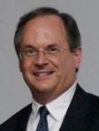 Charlie
Baecker, Lecturer, Entrepreneurship and Strategy, Administrative Director,
The Don Beall Center for Innovation and Entrepreneurship The Paul Merage
School of Business. Charlie
Baecker, Lecturer, Entrepreneurship and Strategy, Administrative Director,
The Don Beall Center for Innovation and Entrepreneurship The Paul Merage
School of Business.
Panelist
Bio:
or over 25 years Mr. Baecker has been involved with new technology-based
ventures either as founder, key employee, investor or board member in both
service and product-oriented companies. In 1987, he founded Assembly
Technologies Corporation providing electronics contract manufacturing
services to the Southern California aerospace, computer and medical device
industries. In 1989 he sold the company and joined start-up Integrated
Inference Machines, working on the development of high-performance symbolic
computation engines designed for use in demanding defense, aerospace and
communications applications. In 1992 he joined start-up Wonderware Corp.
where he served as Director of Network Products Sales. As the Acting
Director of the UCIdeas Research Commercialization Program, he is currently
assisting a portfolio of UC Irvine technology companies pursue their
commercialization plans.
|
|
|
|
Knobbe Martens Olson & Bear
LLP

|
 Jarom
Kesler, Partner in the Orange County office of Knobbe Martens Olson & Bear
LLP. Jarom
Kesler, Partner in the Orange County office of Knobbe Martens Olson & Bear
LLP.
Panelist
Bio: Jarom Kesler is a partner in the Knobbe Marten’s Orange
County, California office. He provides guidance on strategic patent
portfolio management, analysis of infringement and invalidity issues, due
diligence, and intellectual property licensing matters. Mr. Kesler’s
practice focuses on the medical device, information technology, and business
method areas. He received a B.S. degree in E.E. from Brigham Young
University and his J.D. from the University of Minnesota Law School. |
|
|
|
University of California,
Irvine
|
 Dr.
Goran Matijasevic is Senior Assistant Vice Chancellor, Alumni and
Constituent Relations and the Executive Director of the Chief Executive
Roundtable at the University of California, Irvine. Dr.
Goran Matijasevic is Senior Assistant Vice Chancellor, Alumni and
Constituent Relations and the Executive Director of the Chief Executive
Roundtable at the University of California, Irvine.
Panelist
Bio: Goran Matijasevic is Senior Assistant Vice Chancellor, Alumni and
Constituent Relations and the Executive Director of the Chief Executive
Roundtable at the University of California, Irvine. In that capacity, he
oversees and advances research collaborations and strategic initiatives
associated with Alumni Association and Roundtable programs. He also serves
as UC Irvine's ambassador to the local and national business community.
Prior to this position, he was director of research development at The Henry
Samueli School of Engineering at UC Irvine, as well as research coordinator
of the Integrated Nanosystems Research Facility, where he worked on
formation of new industry-university and academic collaborations, especially
focusing on new interdisciplinary research initiatives. Prior to UCI, he
worked as a senior engineer at QPlus, a telecommunications start-up company,
and Director of Research at Ormet Technologies, a developer of electronic
materials and technologies. He managed multiple SBIR projects that led to
several industry consortia projects, as well as a license agreement with a
Fortune 100 company. He has 4 U.S. patents, 3 book chapters, and over 40
conference and journal publications. Goran is currently on the OCTANe
(Orange County Technology Action Network) Biomedical Industry Leadership
Council, the board of Southern California Biomedical Council, and the
advisory boards of 2-1-1 Orange County and TriTech SBDC, and the Economic
Development Committee of the Orange County Business Council. He is the 2013
elected President of the University Industry Demonstration Partnership (UIDP),
a national organization working under the auspices of the National Academies
with the purpose of enhancing value of collaborative relationships between
university and industry. Goran also serves on the UCI Calit2 Division
Council, the UCI TechPortal Incubator Oversight Committee, and the MS in
Engineering Management Steering Committee. He has volunteer taught the
Entrepreneurship Course for Scientists and Engineers in the Henry Samueli
School of Engineering for the last 7 years. Goran received his M.S. (’85)
and Ph.D. (’91) degrees from UC Irvine in Electrical and Computer
Engineering and his MBA (’03) from Pepperdine University.
|
|
|
|
Source Scientific.
 |
 Richard
W. Henson, Entrepreneur, Former CEO, Source Scientific, LLC. Richard
W. Henson, Entrepreneur, Former CEO, Source Scientific, LLC.
Panelist
Bio: Richard Henson is the former CEO and one of the founders of Source Scientific,
LLC, a medical instrument and device development firm in Irvine, California.
Here, he and his partners developed original technology used in diagnostics.
Today, Source Scientific develops and manufactures products for many
well-known in-vitro diagnostic, ophthalmic, surgical and medical device
companies. An experienced CEO with public company experience, Richard
has worked with many high-tech firms in biomedical, consumer and critical
power industries. He has a strong combination of technical, sales, marketing
and managerial experience. He spent several years in Europe with Swiss-based
manufacturers of critical power equipment for heavy industrial markets
including nuclear, power generation, oil & gas, petrochemical and
transportation. He has also served as President of Clary Corporation, a
public company that manufactures harsh environment power systems for
medical, military and transportation applications. Mr. Henson also
serves on the CEO Roundtable at UC Irvine and the Octane Board of Directors.
He is an alumnus of the Anderson School of Business at UCLA. He also
attended California State University, Long Beach (CSULB). He has 4 children
and lives in Laguna Beach, California.
|
|
|
|
K5Launch

|
 Ray
Chan Managing Partner, K5Launch. Ray
Chan Managing Partner, K5Launch.
Panelist
Bio: As an active angel investor with a successful 25 year
track record as a king/queen maker, Ray is committed to partnering with
entrepreneurs to lead them to success. Working in tandem with these
entrepreneurs, Ray loves sharing his passion and knowledge with the next
class of game-changers. Ray has extensive experience within the tech startup
industry. Ray is currently a member and Board Member of Tech Coast Angels
and ACE Fund I and II Investment Committee. In 1985, he co-founded NetSoft,
a leader in communications solutions between PCs, mainframes, and AS/400
systems. NetSoft was acquired by NetManage Inc. (NETM). |
|
|
|
|
Open To Everyone
Reception &
Networking
|
|
|
|
|
11th International SoC
Conference Closed.
|
|
|
|
|
|
|
* Program is subject to change.
SoC Conference Organizing Committee, Technical Advisory Board (TAB), and Savant
Company Inc. reserves the rights to revise or modify the SoC Conference program
(the above program) at its sole discretion.
Copyright © 2003-2013 by Savant Company Inc. All
Worldwide Rights Reserved.
Wafer images courtesy of Intel Corporation, Micron Technologies & Altera Corporation.
| |
|